EVAL-ADAU1466Z schematic
Hello,
I need information about the EVAL-ADAU1466Z. In this evaluation board schematic (UG-1135 rev. 0 available on the site) there are some port hanging.
Two are OP_AMP_REF1 and OP_AMP_REF2 (pag. 33-34) connected to the ADA4841. Another one is FILTR connected to the AD1938.
This ports are not connected with anything else in the schematic and are undocumented in the guide or other datasheets.
Thank you for your help.
ad1938
Integrated/Special Purpose A/D Converters
Audio CODECs
Hello rausov,
Which version of the eval board do you have? Can you take a picture where I can read the part number and revision number?
Dave T
Hello DaveThib, this is my board.
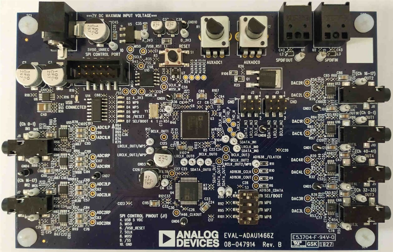
Hello, I have the same question but it seems that nobody has the answer. How did you resolve ? Thank you.
Hello Gino,
Thanks for bringing this up. I had missed the reply to the post from rausov.
This board is exactly the same as the EVAL-ADAU1452RevB board.
Here is a link to the user guide:
EVAL-ADAU1452REVBZ User Guide (Rev. 0) (analog.com)
Dave T
Thank you so much, Dave !
Hello Dave, I am still wondering about the rausov question regarding the scheme at pag 33 of the eval-adau1466z ug-1135 rev.0: I took a look at the document linked by you but the schematic of the input stage is the same, there are still the OP-AMPREF tags routing in the positive inputs of the OP AMPS that are linked to nowhere..and this is so confusing....I am aware that op amps require a bias voltage, and I am pretty sure that these tags matches this task. I measured the voltage on R99 by using my multimeter, it says 3.08V. Is OP AMP REF maybe the same thing as A-3V3 (3.3 V) that comes from the PSU ? Regarding the FILTER tag I found out that it should be grounded through a 10uF capacitor . Am I in the correct direction ? Thank you again.
Hello GinoP72,
In the user guide I linked to is the RevB board and should be the board you have for the 1466.
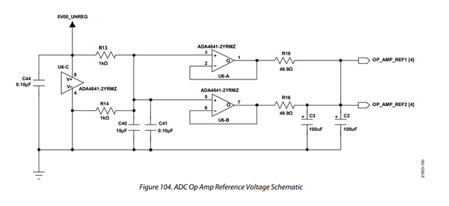
The Op Amp Ref is shown here:
It is dividing down the voltage of the power adaptor feeing the entire unit. The schematic says 5V but we often supply a 6V supply. So 3V is reasonable to measure.
However, I did just notice a mistake in the schematic. I am wondering if it was actually built that way? I will have to check this. It will still work OK due to the 49.9 ohm resistors. This is the mistake:
I circled the connection that should not be there.
Dave T
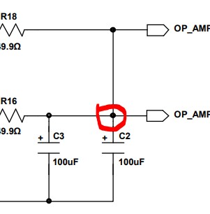
Dave, thank you so much....probably I have misunderstood your first answer: I was expecting to find a different design for the input stage while the missing schematic is in the 1452 datasheet. I agree avout the connection that should not be. I hope that in the schematics provided by AD there are no more mistakes: I’m going to send my schematic for the mastering...
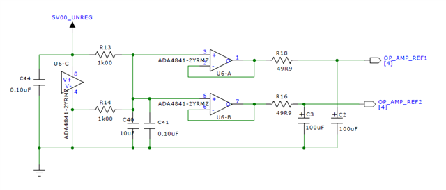
It seems that the schematics were transcribed incorrectly when they were redrawn for the user guide. Attached are the original schematics from the CAD files used to create the board. As you can see, these nets are not connected.
Ken

Thanks Ken!
I am glad it was an error in the user guide rather than the actual design.
Dave T
Thank you very much Ken ! This will be very useful. About the FILTER output: do you agree that it must be grounded through a 10uF cap ?
For the schematics fragment above, the signal is just a filtered, buffered version of the midpoint between the supply voltage and ground. Noise on this signal will directly add to the output signal, so a "large" filter cap is recommended. The exact value will depend on your PSRR requirements.
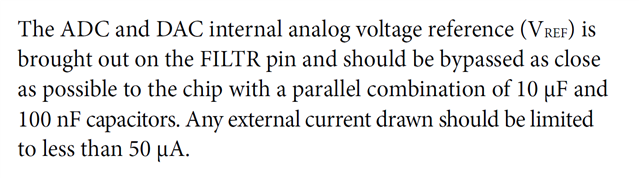
Regarding the FILTR, I used a 47uF cap here instead of 10uF, but the latter is recommended in the CODEC data sheet:
Hello Ken and GinoP72,
I recall having a conversation about this years ago with another Apps engineer that was involved more closely with the original design team. He had said that we recommended the 10uf because the cost was less and the board space requirement was less. This was to not lose business because a customer would think that they HAVE to use a 47uf cap. So the minimum value was chosen to provide good filtering with lower costs. Going up to 47uf will improve the filtering of the CM voltage.
Dave T
Thank you for the update,Dave. I ‘ve just sent the schematic for the making of the master for my board.....cross fingers...:)
Please log in to reply.