Problem with external sync for PCG
Hello all,
I have problems with syncing the PCG to an externa FS. In our System we have the 21469 connected over a SPORT via TDM to an FPGA. The FPGA is creating the bitclock and the framesync for the TDM connection and the mclock for the PCG. The DSP is also connected to an codec (AD1939) via I2S. The clock and FS for the connection to the codec is generated by the PCGA.
We need the codec and the TDM to run synchronusly.
The mclk is SRU routed to the PCG_EXTA_I and the framesync to PCG_SYNC_CLKA_I.
In the PCG_SYNC1 the FSA_SYNC bit is set. (Also tried to set CLKA_SYNC and FSA_SYNC together)
But the PCG does not generate clock and fs. If I remove the FSA_SYNC Bit the PCG runs fine but is of course not in sync with the the TDM.
Do you have an idea what part of configuration I could have wrong that the PCGA is not running when in external sync mode?
Best regards,
Frank
Hi Frank,
The PCG synchronization can be achieved using PCG_SYNC_CLKx_I singal. The PCG_SYNC1 & 2 register allows programs to synchronize the clock frame sync units with external frame syncs. For instance, if FSA_SYNC and FSB_SYNC bits of the PCG_SYNC1 register is set, then the Frame Sync A and B will be synchronized with the External Frame Sync signal given to PCG_SYNC_CLKx via SRU.
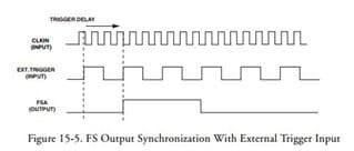
The trigger with the external clock is enabled by setting bits 0 and 16 of the PCG_SYNC register. The phase must be programmed to 3, so that the rising edge of the external clock is in sync with the frame sync.
Programming should occur in the following order.
1. Program the PCG_SYNC and the PCG_CTLA0–1, PCG_CTLB0–1 registers appropriately.
2. Enable clock or frame sync, or both.
Since the rising edge of the external clock is used to synchronize with the frame sync, the frame sync output is not generated until a rising edge of the external clock is sensed.
The time delay between the rising trigger edge and the start of SCLK/FS varies between 2.5 to 3.5 input clock periods. If the input clock and the trigger signal are synchronous, the delay is 3 input clock periods. The following cases need to be considered:
1. PCLK is the input source. In this case if the given trigger event is synchronous to PCLK, the delay is 3 PCLK periods. If the trigger signal is asynchronous with PCLK, the delay varies from 2.5 PCLK periods to 3.5 PCLK periods. (It depends on whether the trigger edge occurs in the positive half cycle or negative half cycle of PCLK.)
2. CLKIN is the input source. In this case if the given trigger signal is synchronous to CLKIN, the delay is 3 CLKIN periods. But if they are asynchronous to CLKIN, the delay can vary between 2.5 CLKIN periods to 3.5 CLKIN periods.
3. SRU is the input source. If the input clock and trigger signal are synchronous, the delay is exactly 3 input clock periods. If asynchronous, it varies between 2.5 to 3.5 input clock periods depending on the phase difference between the input clock and trigger signal.
Please refer the PRECISION CLOCK GENERATOR(695 / 1304) in the below HRM of ADSP-214xx.
www.analog.com/.../ADSP-214xx_hwr_rev1.1.pdf
Can you please share your code snippet to check in my side also Send me the high level block diagram for better understanding.
Regards,
Lalitha.S
Hello Lalitha,
thank you for your answer. I did adjust some small changes related to your description but it did not help for getting my signal. I will attach an document with more details about the current problem.
Regards,
FrankPDF

Hi,
Can you please refer the sample codes for PCG in the below link. Hope this helps.The sample codes for PCG of ADSP-SC58x/2158x processors. Please find the information about each attachment below,
>> PCG is configured to generate clock and FS for I2S using CLK_IN as source clock.
>> PCG is configured to generate clock and FS for I2S using External clock input as source clock
ez.analog.com/.../adsp-sc58x-2158x-pcg-example-codes
Regards,
Lalitha.S
Please log in to reply.