ADAU1701 duplicate power pins
Hello All,
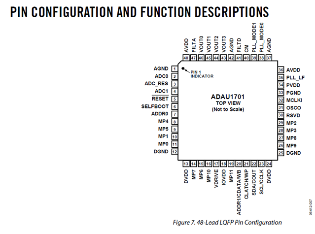
I am currently working on the PCB layout for a board that includes an ADAU1701. However, I am a little confused with the power pins. The chip has a pair of power and ground pins in each corner, 2 for digital and 2 for analog. Do I only need to connect to one of each set with the appropriate bypass caps and leave the other floating?
Kind regards,
Dirk
Audio Signal Processors
pins
SigmaDSP Audio Processors
power
adau1701
Hello Dirk,
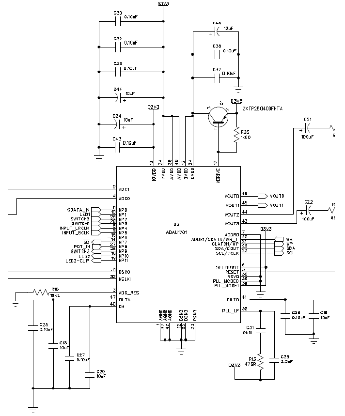
The extra pins share the current and/or provide separate paths to avoid coupling noise between sections -- thus by all means connect them all. Although the ADAU1701MINIZ eval board is not intended to be a reference circuit, we see all of its -1701's power and ground pins connected, as shown below:
You may also find the SigmaDSP Layout Best Practices document helpful. Have fun with your design!
Best regards,
Bob
Hi Bob,
Thank you for your swift reply! I will follow the SigmaDSP Layout Best Practices and switch to the evaluation design should it not fit.
Out of curiosity; the 85 and 60 mA that the ADAU1701 uses on digital and analog does not seem to indicate the need for splitting the current over several power pins. Would the split then be needed for the internals of the ic? Or are they not even connected internally?
Best regards,
Dirk
Hello Dirk,
Questions on the IC's internals would take a ADI engineer to answer. However, we can make some educated guesses. Because the -1701 combines analog and digital circuitry in the same chip, special care is needed to keep digital 'hash' away from the analog circuitry. Likely the digital current draw is not pure DC but has significant ripple. If one pin served for both analog and digital grounds, the ripple current would develop a ripple voltage across the common bonding wire and pad within the package -- injecting this ripple into the analog circuitry. And it doesn't take much. For argument, suppose the ripple was 10 mA p-p and the common ground resistance 10 milliohms. The shared ground pin would then add 100uV p-p noise to the analog output-- enough to limit the s/n to 90 dB. Keeping these separate until connected outside the chip eliminates this shared path.
Best regards,
Bob
Please log in to reply.