Analog Devices 14 Bit ADC (AD9640BCPZ-150) Distorted Sampled Output
Hi Friends,
I have designed a board which has AD9640BCPZ-150 analog to digital converter from Analog Devices.
This ADC is interfaced to a Spartan3AN FPGA. The ADC is seemingly producing distorted output (or call it missing code problem). The detail of this trouble is as under:
Trouble Description: The captured analog data produced by any channel of this AD9640 has distortion. This distortion is produced by the steps that are suddenly introduced in the output data at some particular voltage levels. The schematic of our AD9640 interface can be found in attached “Schematic.pdf”.
I have verified the integrity of all data, clocks and control signals between ADC and FPGA and I do not find any trouble in it.
I have performed a test. In this test I generated the differential Sawtooth Signal from on board 14Bit , DAC2904 DAC and connected the output of this DAC to the input of this AD9640 in following fashion:
ADC_D_A+ = DAC_D+
ADC_D_A- = DAC_D-
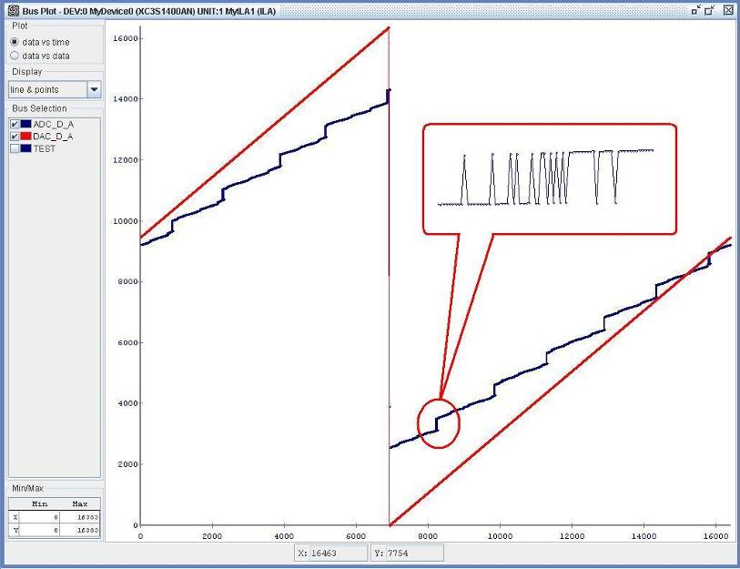
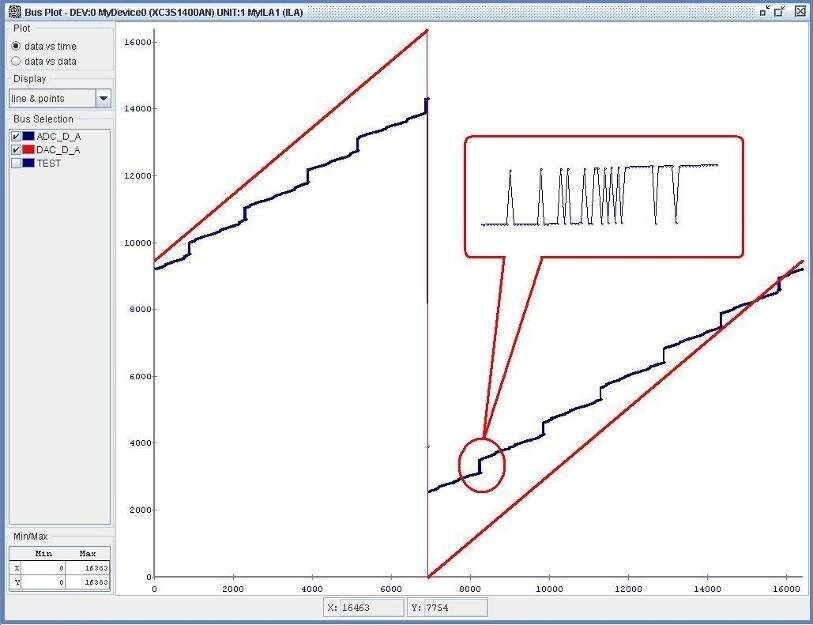
In following picture you can see the Output of the 14 bit DAC captured through Xilinx Chipscope pro in RED color. and the captured output of the AD9640 channel A in Blue color.
Busplot.jpg:
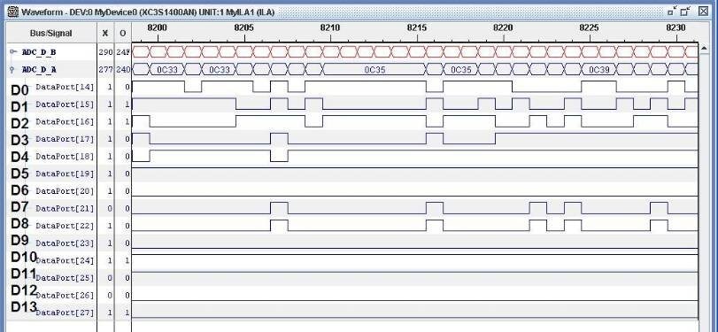
Dataview.jpg:
I ran the test on our other boards as well (same design containing AD9640BCPZ-150 ICs), but the result is same. That is we see sudden steps in the sampled ADC output, regardless of the ADC channel being monitored. We have this problem on 10 prototype boards that every AD9640 ic on these boards produces sudden steps.
The ADC is initialized on powerup to produce Offset Binary codes. However I also ran the ADC in 2's complement format (by writing through SPI to the control register). In 2's complement mode the output format changes but these small steps still can be seen.
In this above mentioned test the scheme uses a dc coupled connection between the DAC output and AD9640 input.
In this test the DAC produced a saw-tooth wave by running a 14 bit counter inside the FPGA that samples ADC channel A on ADC_DCOA clock signal (at 25MHz).
The file dataview.jpg shows the step (shown in red circle) is actually caused by a simultaneous motion of D7 and D8 bits, which start to toggle at this location simultaneously. This behavior we can observe at multiple locations of these sudden steps. And some times the bits that start to toggle simultaneously are D6 and D7 and some times some other consecutive bits.
The captured data can be found in “busplot.txt”
The schematic of the AD9640 can be found in “Schematic.Pdf”
The response is same (that is sudden steps are observed) even if i have AC coupled connecting through AD8352 differential amplifier, as i had performed another test by feeding ADC with a sine wave from external function generator.To add more details here I have observed that these steps are not related with the sampling frequency or frequency of the input signal fed to the ADC. Rather they depends on the voltage level at the ADC input. if i increase sampling frequency i still see as many steps as they were before. and if i increase ADC input signals frequency even then these number of steps remain unchanged. The only thing that changes the number of steps is the peak to peak voltage of the input signal fed to the ADC. if i decrease the input voltage i see less steps.
I request you to please suggest whats wrong with this ADC chip. Looking forward for your reply,
Thanks and Best regards,
Asim
adc
amplifiers
code
Fully Differential Amplifiers
Differential Amplifiers and ADC Drivers
distorted
ad8352
ad9640
missing
output
High Speed A/D Converters >10 MSPS
non-linearity
Standard High Speed A/D Converters
Show More

Hi Asim,
As your question pertains to an ADC, I should advise that the EngineerZone is currently for the support of Analog Devices DSPs only. While someone on the forum may be able to offer assistance on this topic, I would recommend that you follow the correct support channel from the following link:
regards,
Craig.
Hi Friends,
I am desparately waiting for answer on my post. I 'd welcome any suggestion.
Would someone help me resolve the trouble i am having with AD9640 device.
If there are any questions related with the AD9640, that you think I should answer I would love to answer them as well.
Best Regards,
Asim
Thanks Craig,
I have already contacted people at cic.asia@analog.com and cic@analog.com.
People at cic@analog.com say that for this product only people in china (cic.asia@analog.com) will support you.
However the reply that I had received from china does not contains answer that can help me resove the issue.
They just stated that the Device AD9640 chip gaurantees no missing codes and suggested me that i should look at my hardware.
I had posted in this forum in a desperate hope that someone might answer to the problem i am having.
Regards,
Asim
Hi Asim,
I spoke with a colleague who supports this ADC. They had some comments regarding your schematics, which I hope will be of assistance to you:
Looking at your schematic the RBIAS resistor, R6, is set to 1K. This resistor must be set to 10K. With this resistor value set incorrectly the internal bias currents are incorrect and this is likely causing your issue. I also noticed you have 2 0.1uF capacitors on the VREF node, one of these should be changed to a 1.0uF capacitor. There is also a note on the schematic referring to a power supply sequence requirement for the AD9640 - this sequence is no longer required - refer to the AD9640 revision B datasheet. Lastly, I have attached the AD9640 eval board schematic.
regards,
Craig.
Great, thanks for letting us know. I'll pass on your comments.
regards,
Craig.
Hi Craig,
And thank you so much.
I changed the RBIAS resistor from 1K to 10K and it fixed the problem. Now I dont see those sudden steps in the data captured by AD9640.
Next I am going to increase the value of capacitor from .1uf to 1uf as you suggested.
I am really greatful to you for helping me. Also please pass my kind regards to your colleague who pointed out this RBIAS resistor value.
Best regards,
Asim
Adding as a note for future reference for anyone reading this thread:
The purpose of the EngineerZone is to provide forums for the support of Developers using ADI DSPs and related tools. Those looking for support on non-DSP products should see the Analog Devices Support page, via the link below, for details of the appropriate contact:
regards,
craig.
Hi Craig,
Is there a plan to the future to add new groups in this forum?
E.g. the ADC/DAC part, or RF part caring about Analog Devices part of course.
Regards,
Afi
Hi Afi,
We are constantly evaluating EngineerZone and may be adding support for other Analog Devices products in the future, but right now we are only supporting ADI's embedded processors and DSPs through the forum. We will post any news about forum changes or additions to our spotlight blog at:
https://ez.analog.com/blogs/engineerzone-spotlight.
You can receive an email notification when a new blog is posted by clicking "Watch this blog" from the blog page.
regards,
Craig.
Please log in to reply.