OFFSET VOLTAGE AT AD1938 CODEC DAC OUTPUT
Hi Support Team,
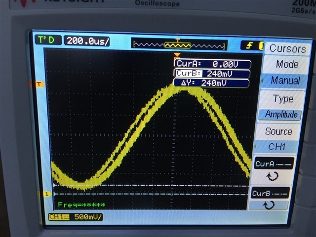
I have EVAL-ADAU1466 Board and I'measuring 240mvDC offset at DAC outputs.Why I'm having such a big offset voltage and is there a way to eliminate this offset voltage at DAC1L(TP75) and DAC1R(TP68) ?.
Regards,
Edit Notes
Image is added
[edited by: Husnu at 7:01 AM (GMT -5) on 7 Mar 2022]
ad1938
Integrated/Special Purpose A/D Converters
Audio CODECs
Hello Husnu,
I hope adding a DC blocking filter before DAC in your program will eliminate the DC offset. It is located under Filter>>Miscellaneous filters>> DC blocking. Please try this and get back to us.
To eliminate DC offset in ADC, In Codec Register controls>>In ADC control, you can find the feature of enabling HPF. The cutoff frequency is around 1Hz. So it will remove the DC offset so it is not a problem with any filtering or other DSP processing.
Regards,
Harish
Hi Harish,
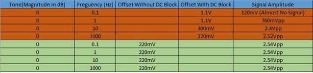
I tried with DC Block and without DC Block and attached Project file and results as table. For higher frequencies it does not make any difference, for low frequencies even it worses.
SchematicDCBlock.dspproj
As you notice my sampling rate is 192KHz. I have tried with 48Khz either, nothing is different.
Looking to hear you.
Kind Regards.
Husnu.
Hello Hasnu,
From your screenshot, is this the offset you are talking about?
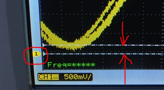
So is cursor 1 set to the level of ground?
This is not a DC offset.
The output of the DAC is not centered on 0VDC. It is centered about a common mode voltage of around 1.5V. Then the DAC goes positive or negative from there to produce a sine wave. the positive and negative peaks of the signal will never reach 3.3V or ground because there has to be some headroom and the drive circuits cannot go exactly to each power rail. If you shut off the sine wave by muting in the DSP you will see that the output is sitting at around 1.5V.
So you are sending what is probably a full scale digital signal and the negative peak is not quite going all the way to ground. This is no problem at all and is how it is designed. This is why most people cap couple the output of the DAC and it is done that way on the eval board. If you look at the test point "OUT L" you will see the sine wave centered around 0VDC instead of around 1.5V DC.
Dave T
Hi Dave,
I hope you're doing well.
Curser1 is set to ground. Cursor2 is set to bottom of sine wave with 0 db offset. I'm aware of that when you generate a signal with 0 offset I have signal around 1.5V before output cap and have signal centered zero(GND) after output cap, because cap eliminates DC voltages. What I'm expecting is when we generate a sign wave from DSP is negative peak touches to GND and positive peak is some where above center point at DAC output. I need to generate signal that negative peak or lowest point will touch to ground without any distortion. So my understanding from your explenation is it's design intend and I'll add extra circuitry off the eval board to eliminate this output offset any way. I have never seen any square, tone or triangular way even with lowest negative offset touching to ground. All signals negative peaks touches to 0.24V. I'm not clear if I connect different CODECs other than AD193Xs to ADAUDSP will I get the same result. I wonder 0.24V is originated from CODEC or DSP. When I try different board with FPU and DAC(10Bit resolution) inside I have pure signal negative peak touches GND.
I have seen some document ( looking for it and never seen yet again) about this situation which says that to eliminate this problem GND should be replaced with more negative voltages around -0.275V., so negative rail touches to GND.
I'll look for your further suggestions that helps.
Kind Regards.
Hi Husnu,
Dave's answer is correct.
The AD1938 is designed with audio applications in mind. The DAC output will *not* extend all the way down to 0V with the standard application circuit. The AD1938 is not a rail-to-rail DAC, it is optimized for AC performance.
Now let's look at the datasheet (page 3) to show that this is expected. As you have found, the output voltage is centered around the common-mode bias voltage, 1.5V.
From here, the full-scale range of the DAC is specced at 2.48Vpp. So 1.24V above and 1.24V below 1.5V.
A fully negative signal will therefore create 0.26V which matches your result.
You can further condition the DAC output to move the offset yourself, or, switch to a DAC with the DC specs you need.
Best regards,
Joshua
Hi Joshua,
it's very clear that DAC output is centered exactly at 1.5 V, and there's 0.230 V offset voltage anyway. I have added off the board circuitry and solved my problem. Thanks to Dave and you for your cooperation. I will accept yours explanation as answer.
Kind Regards.
Please log in to reply.