ADAU1701 Schematic helpful guideance
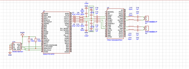
Hello, I am posting here as I am inexperienced in circuit design, and I am basing a design for a Stereo amplifier off of the ADAU1701 DSP, and Texas Instruments TPA3118D2 amplifier. Attached below is a screenshot of the circuit as it stands currently. Guidance or tips/tricks would be greatly appreciated to help me achieve the end goal. Namely, the Self-Boot typical application schematic in the data-sheet for ADAU1701 labels 2 resistors (R7,R8; Referenced as R9,R10 in attached schematic) with values of 2K20. Im not exactly sure what I would use to match these values, or if those values are generic and need to be adjusted for a specific use case. Thank you ahead of time for your patience and willingness to help someone who is basically a foreigner to this domain.
Audio Signal Processors
hardware
schematic
SigmaDSP Audio Processors
adau1701
Hello DPicarazzi,
Looks like a great design. I would love to see one of our amplifiers but I am happy you are using the DSP.
The resistors R9 and R10 are the pull up resistors for the I2C communications bus. Phillips Corporation has plenty of documentation for the standard but it gets a bit complicated. We recommend 2.2K which is on the lower side. Generally they are around 2K to 4K and often I see them in the 3K range. 10K is rather weak. This will effect the rise time of the data. It can slow down things like the ACK and cause data errors. It will effect the speed that you can run the communications between the EEPROM and the DSP.
In the USBi we use a 10k pullup as a weak backup in case you plug it into a circuit that does not have any pull ups. So it would have at least 10k and if the circuit has a 2K then a 10k additional pull up will not change the total pull up by much. So it will most likely work with the 10K you have but I would use something closer to what we recommend in the datasheet.
Dave T
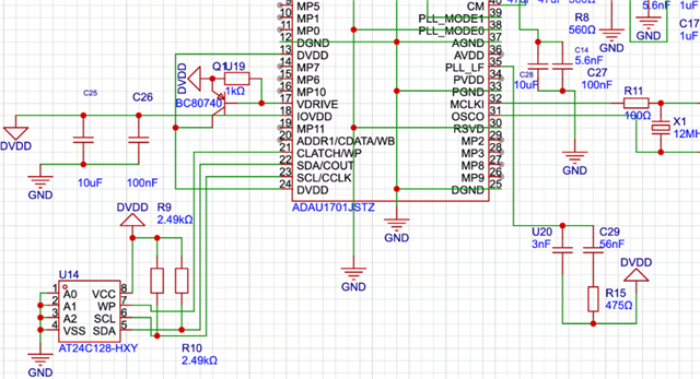
I would love to use an ADI amplifier, but I haven't seen any that accept an analog input that I could incorporate as a drop in replacement for the TI amplifier in the schematic. If there is one I'd love to know so I can drop it in to this project! Now in the data sheet, the selfboot schematic shows a writeback circuit. What does this circuit consist of? Attached is an updated version of the schematic for anyone to check and make sure that it is correct

Hello DPicarazzi,
Hoe much power do you need? What is the speaker impedance? Does it have to be analog input?
There are a lot of little thing regarding power that is either missing from the schematic you posted or wrong. So of it is the name you assigned to the DVDD power net.
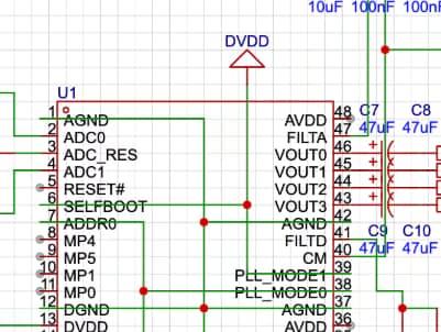
AVDD does not seem to be connected. This needs to be connected.
Selfboot is held high. This is OK and is mentioned in the datasheet that you can tie it high but it is best to pull it up with something like a 1K resistor. Then either put some pads or a header such that you can easily ground the pin to defeat the selfboot when working on the program. It can cause some issues when using SigmaStudio to develop the program.
Reset pin does not seem to be terminated. This should also be pulled up and have a small cap to keep noise off of the pin. 100nf is fine and I have seen some people use 10nf.
ADDR1 is floating. You need to tie this high or low. Usually most people will set the address of the part as zero so pull it low.
IOVDD pin is tied to a net you are calling DVDD. Then the DVDD regulator output you directly connect to the DVDD pins and you do not give it a net name so the actual connections seem fine, it is just confusing. I would change the netname DVDD to either IOVDD or AVDD.
The loop filter needs to be decoupled to AVDD, you have it using the IOVDD (DVDD in your drawing) and you have nothing connected to AVDD so I assume you will tie your net name DVDD to the AVDD pin. See how using the name DVDD creates a lot of confusion.
Pin 21, the CLATCH/WP pin. You have this directly connected to the EEPROM. This pin is an open collector when in selfboot mode so you need to pull this up to the IOVDD to ensure it sits high.
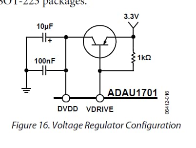
You have no bypass and filter caps on the DVDD regulator output. These need to be added.
The Writeback feature and circuit is a little difficult to implement and I do not have a good example to point you to.
The first step is to have a logic signal developed that signals that power is going down. Sometimes a Power-Good signal from a regulator can serve as this but timing becomes super important. Once power is going down, you need to have some diode isolation and some large filter caps on the power to keep it up long enough from when the logic signal triggers "power-going-down" to allow the DSP to react, pull the WP pin high, and write eight values into the EEPROM and compete this all before power is actually gone. This is not trivial and lots of things to consider like how long will it take to do the write to the EEPROM, how much capacitance can I put into the circuit to hold it up long enough to sustain the power draw of the DSP so it can complete the writeback. This will depend on your circuit.
The circuit on the WP pin needs to allow for the DSP to be able to pull this high and you need to be able to pull this high when you need to program the EEPROM and I assume you would want to have this pulled low the rest of the time to protect the EEPROM from being written to. So many little details. Tough for someone just starting out to work out all these details.
Dave T
Please log in to reply.