ADAU1787 Eval Board Source Files
Hey ADI,
I'm currently working on a product involving the ADAU1787.
Are you able to provide the source design files for the ADAU1787 Eval board (ie - Altium, Orcad, PADS, etc)? If not, are you able to provide the ODB++ or Gerber files for the eval board?
Would help as we begin to layout our board to see what was done with the eval board.
Thanks!
hardware
ADAU1787
altium
Integrated/Special Purpose A/D Converters
SigmaDSP Audio Processors
layout
ADAU1787 evaluation board
EVAL-ADAU1787Z
pcb layout
Audio CODECs
Show More
Looking for some recommendations for via sizes and fanout guidelines for interior pins of the BGA which is why I'm asking for the source files. Saw there were questions asked here but there weren't really any answers to the questions posted and the eval board user guide doesn't seem to have more information on the fabrication details: Trace routing for ADAU1787
I see layer stackups but not much information beyond that.
Tagging DaveThib as I thought you might be able to speak to this more.
Zach,
Please see attached fab files, and let us know if anything else is needed. 09-056963-01A.zip
Hello Zach,
I will add one thing to the info that Patrick provided. On our web site we do have some documents that help with layouts.
Here is one: PCB Design Considerations and Guidelines for 0.4mm and 0.5mm WLPs | Analog Devices
Dave T
Thanks so much!
Thanks Dave!
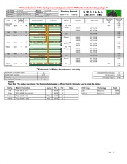
Hey galvinpjg and DaveThib - I've attached a couple of files from what you had sent. Is there any reason why layer 5 in the stackup is blank? Is there some esoteric reasons (noise, RF immunity, etc)?
PDFPDF
Hello Zach,
That is a very good question. I do not know the answer. I was not involved in the design of this eval board. Patrick might know but I think this board may have been designed by our global design resources and in that case it might be hard to find the answer. It may be simply that it was not needed for any signal routing so doing something like just adding another ground or power plane would add a fair amount of capacitance so that might be the thinking here...
Dave T
Ok gotcha - from what me and my colleagues see, this is a very unusual PCB stackup, and we might get some resistance from board houses when we go to have our board made. If there are very legit reasons for it, then we can fight our fight with our board, but I would like to understand more if possible. Are you or galvinpjg able to dig and find out some more info on this?
Zach,
Layer 5 should be a copper layer. So it is not blank per se. PDF's of the layers 5 is here. PDF
Hello Zach,
Patrick and I talked about this and you can see his new post with the PDF. It looks like the layer was a plane and it should be tied to ground. With a signal layer close by it would be good to have it be grounded for signal integrity (impedance) reasons.
So you will not need to go through hoops to make the layer blank. I agree, it would be strange and difficult.
We suspect the stackup document is somewhat in error. It says it is copper foil yet no plating. Perhaps they just left the foil as is and did not bother to plate it to a thicker layer. I would certainly lean towards making it a 0.5oz copper layer.
Dave T
Great - that helps a ton. Thanks for the info both of you!
Hey galvinpjg - my engineer just noted that the layer 5 PDF above is noted Rev 0, but the fab files provided by you on December 10 have Rev 1 files. The eval board that I have is also Rev 1.
Can you clarify that we can trust that Rev 0 for layer 5 is the same as Rev 1 and is current/hasn't been updated? Or provide Rev 1 of layer 5 just so we are 100% with knowing we have our layer stackup and geometries correct?
DaveThib just checking back in here to make sure my question didn't get lost over the holiday weekend.
Hi,
DaveThib Can you provide deeper info on the stackup ? Are they doing stacked 4/8 mils uvias from L1 to L4 ? I guess uvias are inevitable, Am I correct ?
Please log in to reply.