ADAU1452/1466 - Bypass, Decoupling, PLL and reservoirs
Hello!
Im trying to design a PCB with either the ADAU1452 or the 1466. Im fairly new to PCB design so excuse my ignorance :)
I have been reading far and wide about decoupling and bypass caps and it seems there are many interpretations of whats right or wrong.. Searched this forum and found these links:
SigmaDSP PCB Layout Best Practices
Question about ADAU1452 PCB layout
I also looked closely at the datasheets of the chips as well as the eval boarsd.. But I didn't quite find my answer.
Im a bit confused about the placement of VIA's and bulk capacitors.
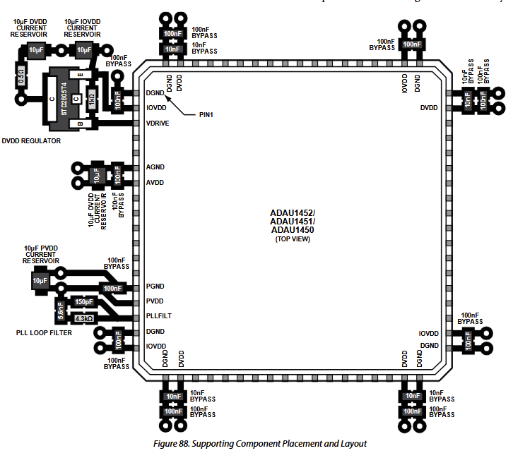
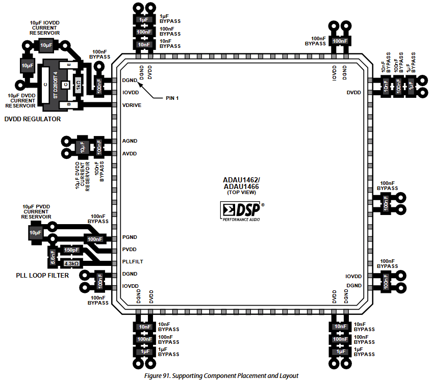
Looking at the datasheet of the two chips it seems pretty straight forward. Just put the caps close to the pads and then the VIA's on the outside. But why are the 1 uf reservoirs not shown on 1452? Also what is that bypass shown on the middle of the right side on 1466? is that a mistake in the datasheet?
Question 1 - Decoupling caps and Vias
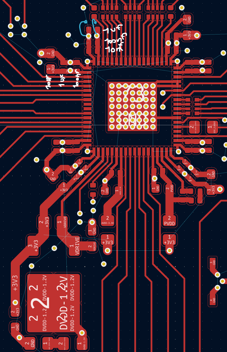
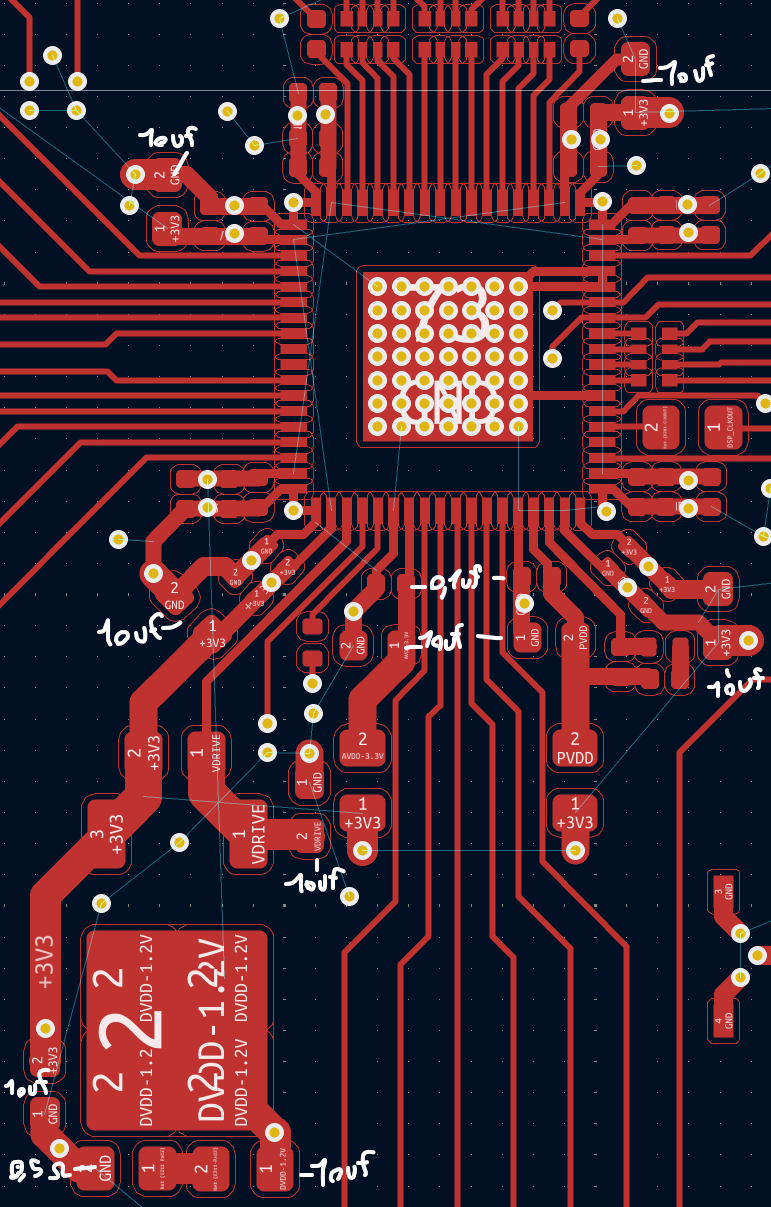
Is a layout like this somewhat decent or did i make some stupid mistakes? This wont be the last PCB i do with these chips, so I would like to learn how to do it the best way and not just good enough. :)
Should the vias rather be placed on the outside of the 1 uf caps like in the image in the datasheet? or is this better? Also on the Eval board the layout is again quite different. There are no traces on the GND side of the caps only Vias, and no 1uf is this better?
Are all of these versions actually equally good and im just overthinking it? (EDIT: There are a few GND vias missing on my PCB at the 10 uF caps - ignore that)
Question 2 - Bulk/reservoir caps
Something that isn't really covered in the datasheet (probably because it is common knowledge when you know how to make PCB's) is the placement of the 10-47uF reservoirs. In my design i chose ceramic as thats whats used on the eval board. This also means i have the 0.5Ohm resiostor in series with the dvdd one. Is there a benefit of using electrolytes instead? or are ceramics okay?
Right know i placed one 10uF at every pad like this for a total of 40uF:
Is it ok to place one at each pad like this? or should I only use one pr named rail as it is stated in the datasheet? in that case, where should i place it? at one of the pads as above or further away?
Question 3 - Pll circuit
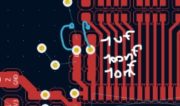
Is this PLL circuit decent or did i mess up somewhere?
Question 4 - Termination resistors
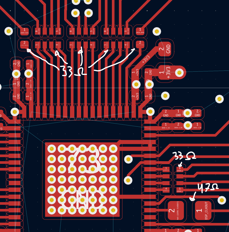
I have read that termination resistors should be as close to the outputs as possible. therefore i have chosen 33 ohm 0402 resistors that I cannot replace by hand. therefore i just want to double check that its a decent choice (based on eval baord)
I saw another application where they placed resistors on the EEPROM lines, are these really a good idea or not? They are not used on the Eval.
Sorry for all these questions, as mentioned I'm new to PCB design and just want to make sure I get it right!
Best regards, Daniel
Edit Notes
Small mistakes
[edited by: DannerD3H at 10:44 AM (GMT -5) on 15 Dec 2024]
Audio Signal Processors
adau1452
hardware
decoupling
pcb
SigmaDSP Audio Processors
layout
bypass
pcb layout
adau1466
Show More

Hello Daniel,
You have a ton of questions. I will do my best to get through them.
First, yes, the stray cap on the right side of the 1466 datasheet layout example is an error in the datasheet.
Before I get too far I also need to mention that you will want to refer to the ADAU1452 RevD datasheet for the common elements between the ADAU1452 and ADAU1467 family of parts. I had put in a lot of work to update that datasheet back in 2018 and a lot of it was with the voltage regulator for the DVDD when I worked with the designer of the regulator before he retired to come up with the changes. It was a situation where the electronics industry has improved?...Changed?.. whatever you want to call it people are not using 10uf electrolytic capacitors as often since ceramic ones are now available at a reasonable cost but were not when this part was first designed.
The other detail is that these PCBs were not designed by me. I was a little involved with the RevB board but not a lot.
I was consulted when the codec did not meet specifications and I advised on the layout of the codec and that fixed the codec performance issue but I was not consulted on the DSP part of the layout. The investigations I did with the voltage regulator all happened after all the eval boards had been designed. So I really do not have a good layout to point to for you to copy. I wish I did. By the way, This is the post and the document I wrote up about the codec PCB layout: (+) PCB Layout Best Practices for AD193x codecs - Q&A - Audio - EngineerZone
The concepts are the same for the DSP.
Question 1:
Yes. move these vias.
You are correct, do not put the ground vias right by the pin. Make the trace to the pin go past a bypass cap before going to the via to the ground plane,
For your question 2 I will expand on a few things.
I am glad you found the detail about the ceramic 10of caps and adding the 0.5ohm resistor. There is no real advantage to using the electrolytics. I think going to the ceramic caps is probably better because they do not dry out over time and change value! The only issue is that the regulator was designed with electrolytic caps in mind and the ESR of the cap is a real factor in the phase margin of the regulator. That is why you need to add the resistor in series with the ceramic cap.
Notice that the ADAU1452 newer datasheet does not have the 1uf caps. This is because in simulation this reduced the phase margin. Do not use the 1uf caps and certainly do not add more than one 10uf cap. Having several 10uf caps will reduce the phase margin. The 10uf cap is for larger and longer lasting current demands so the placement is not as critical because there will not be as much of a high frequency "edge" to the demand so the inductance of the vias do not make a difference. The 100nf caps are the ones that handle keeping the short high frequency clock and data edges from becoming a problem. The caps work both ways, they keep the noise generated internally in the part from going out onto the power and ground planes and it also reduces any noise that happens to be on the power and ground planes from getting into the part. I would follow these bypass cap and via placement everywhere in your design.
I do want to add one thing here. There is no such thing as a perfect PCB layout! You always have to make compromises somewhere in the design. I feel that understanding that you are making a compromise will help you minimize the bad effects and be on the lookout for issues once the PCB in in hand and being tested. As you have noted, our PCBs are certainly not perfect yet they work decently well.
One other detail. When I was doing this analysis work I went into the lab and TRIED to make the regulator unstable by adding a lot of extra capacitance, and I mean a lot, and I was never able to get it to be unstable. So the design is good and the simulations are all over silicon variations and temperature ranges so my one nominal board at room temperature would not go unstable and oscillate. But, I went with the simulations since I did not have months to experiment with silicon skews and various temperatures.
Question 3,
I think your PLL loop filter placement should be fine. I do not see anything that really stood out to me.
Question 4.
Let's have a bit of fun here today,...What do you mean 0402 resistors are not replaceable by hand? About a two years ago I had to replace some sitting on my knees behind an audio console with poor light and only a large SMT tweezer and standard soldering iron tips! I got it done! But,... it was not pretty! We do this in the lab here at ADI a lot but we have small tweezers and a microscope!! Even then it is still tough. So I get it! with my personal designs I do for "fun" I do not even use 0603, All of my resistors are 0805 so they are replaceable by mere mortals!
That said, you really do need to use 0402 because you want to minimize the trace lengths and few turns and curves. Yes, these resistors are a great idea and I would for sure add them. They are best placed near the source but this can be one of those trade-offs I mentioned. It is better to have a more direct and shorter signal path than to have the resistor close to the source. Try your best to do it and it looks like you did a great job.
Regarding on the SPI lines. That is a tougher question. If you are going to try to run as fast as possible with the SPI then yes, add the resistors. For our eval boards we only boot up from it and usually we use 10MHz at the most so the damping resistors are not as critical to be there. If you are going to use a RAM chip to do external delay lines then you will have to push the speed so then damping resistors will be important. You will be increasing the drive strength of the output pins which will make the transmission line ring more.
So if you only have an EEPROM for booting up the DSP and you do not need to boot up as fast as possible then do not worry about the damping resistors.
Well, This is my book for the day. LOL
Sorry this was a little long. I obviously like talking about this stuff too much!
Dave T
Hey David,
Yes I am sorry for the long list of questions.. Im totally new to all this stuff and just trying to understand as best as I can. I really appreciate you taking your time to write such an extensive answer covering all my points!
Thanks for the tip on the datasheet. I didn't considder looking at the revision table of the two.. I will refer primarily to the 1452 then.
Im also happy that you say the Eval board isn't the ideal design. That took a lot of confusion off my shoulders! Especially compared with you good examples in the link you provided. Thanks!
So to summarize, just to make sure I got everything right:
Remove the 1uF caps on all the power pins and only use 100nF with the addition of 10nf on all the DVDD pins.
Only add one 10uf ceramic capacitor to each named rail. no more, no less.
It is okay to decouple the PLL supply (PVDDD) and the AVDD with ferite beads as shown? - I have seen this done on another DSP design using the 1452.
I2S resistor placement is okay - and no, mortals cannot desolder 0402 resistors, only gurus ;)
The resistors on the EEPROM lines are meaningless for boot up only, but do no harm?
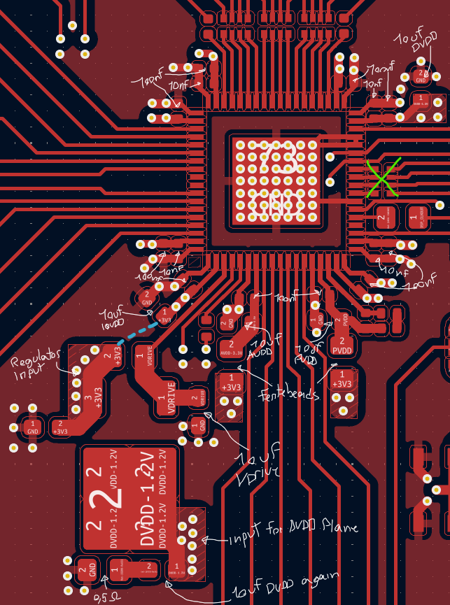
This is the updated layout with now only one 10uF at each rail and no 1uF caps. Also I added some more vias and pours around the ferite beads and DVDD regulator. Does these make any sense or should I stay with a single via everywhere?
I also removed the trace (now dodded blue line) from connecting a IOVDD pad to the 3.3v input of the regulator. This is shown in the datasheet, but am I right that it doesn't mean it actiually needs a trace but just needs to connect to the same net?
Also the extra 10uF cap shown at the regulator for the DVDD net. I suppose this is not the required bulk capacitor needed at the chip? meaning there are actually supposed to be two 10uf caps on the DVDD net as in my current layout. Or am I wong? I chose to place the other 10uF as far away from the regulator one to sperad out the supplies.
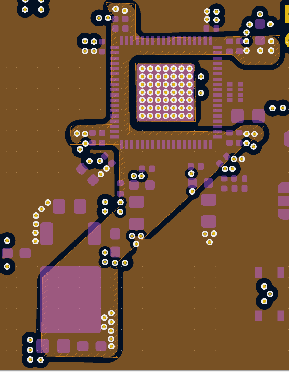
FIY. this is the power plane on layer 3 (Layer 2 is pure GND).
Again, thakyou very much for taking your time answering all these noob questions! I don't mind it beeing long, share all you are willing to share! I'm a dry sponge at the moment :D
Best regards, Daniel
Hello Daniel,
DannerD3H said:
So to summarize, just to make sure I got everything right:
Remove the 1uF caps on all the power pins and only use 100nF with the addition of 10nf on all the DVDD pins.
Only add one 10uf ceramic capacitor to each named rail. no more, no less.
It is okay to decouple the PLL supply (PVDDD) and the AVDD with ferite beads as shown? - I have seen this done on another DSP design using the 1452.
I2S resistor placement is okay - and no, mortals cannot desolder 0402 resistors, only gurus ;)
The resistors on the EEPROM lines are meaningless for boot up only, but do no harm?
1) Yes, remove the 1uf. The 10nf are your choice. Not a big difference with them in or out when it comes to phase margin and I could only see a slight difference with the noise waveform on the pin when I did these tests in the lab.
2) Yes.
3) Yes, ferrite beads are OK as long as there are bypass caps on both sides and usually there are.
4) Give yourself some credit, some good equipment and a decade or two more experience and you will have it mastered!
5) The resistors are a good idea but usually not needed unless you are pushing the speed of the EEPROM up towards the max. So basically, yes, they do no harm.
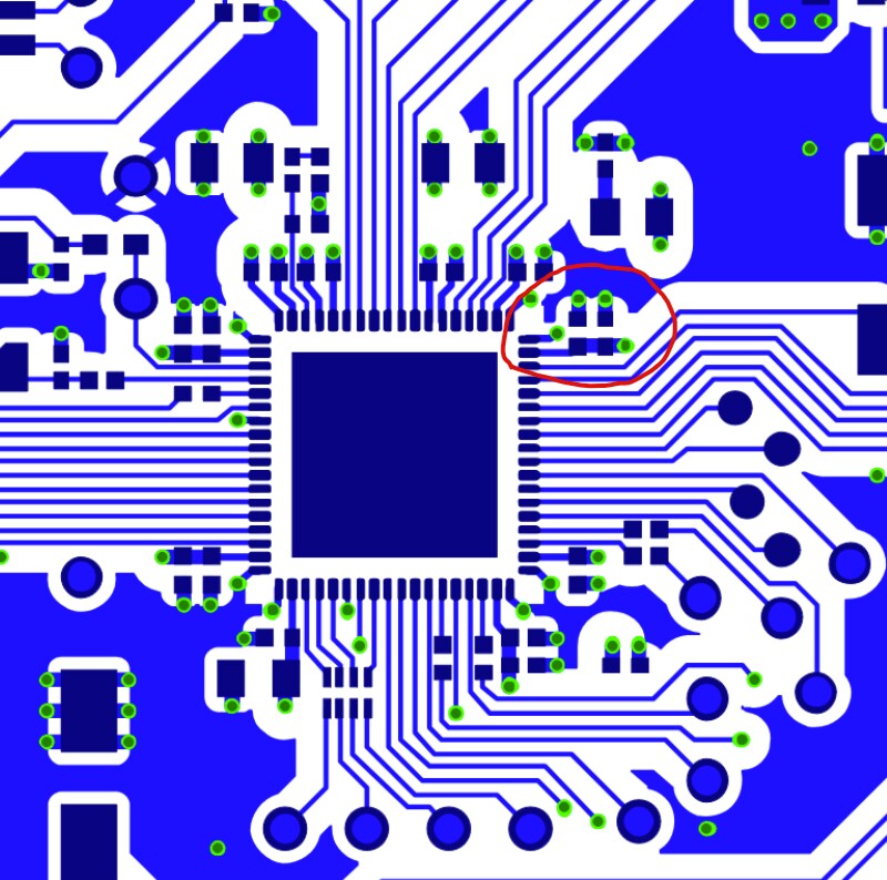
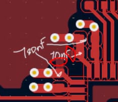
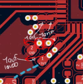
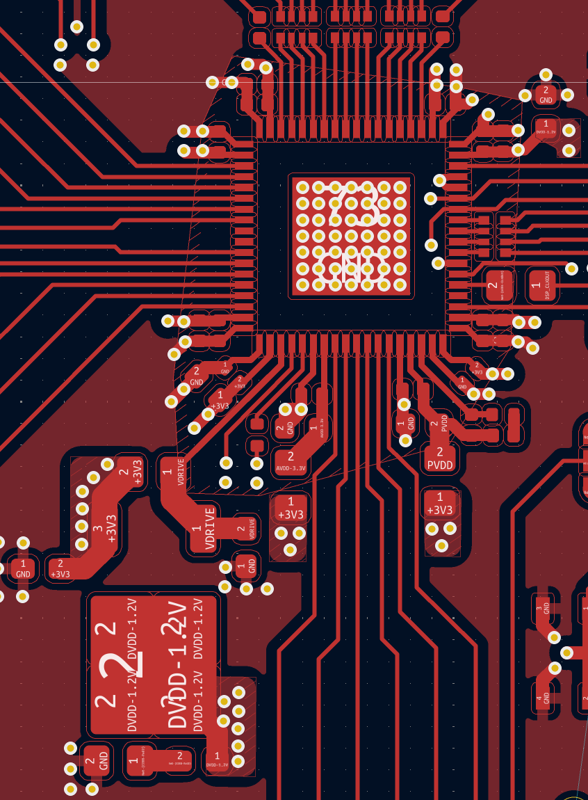
Now I am going to start getting more picky. The ground fill on the top layer should not be allowed to touch a pin or a pad unless there is a via right there to the ground plane. Here is an example. Stop (block) the fill from getting to these pads:
Next:
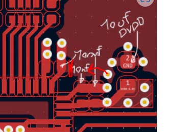
A few comments about this area:
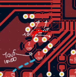
See where I added the red scribble? Get rid of the ground fill there. But there is more... New screenshot:
Even though this is the 10uf cap, I would do this since it is easy to move the vias to the other side.
Next:
On this next place I would remove the ground fill where I noted and move one via to sit closer to the two bypass caps.
Next:
This next set of comments are not super important. Just minor details.
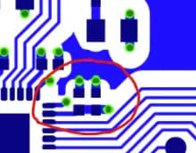
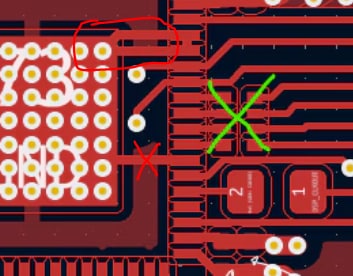
I do not like to see any pins tied to the EP that is under the part. I feel it is best to let that get its ground from all the vias and not tie any of the pins to it. I have seen an issue when someone had tied the PGND and the DGND both to the ground fill on the top of the board and that caused a feedback path between the digital and analog sections of the part and caused the PLL to lose lock! In your case it is not as bad, and not super significant. Here is what I see:
The pin that is tied where I drew a red "X" is a stray DGND pin that is not closely associated with a power pin. However, it will still be tied internally to all the other DGND pins so I would not want to have stray currents or noise from the EP to get into the ground ring in the part. So if it is possible I would give it its own via to ground.
The red circle are two logic pins that are tied to ground via the EP. These are the address pins for the comms port so there will not be a lot of current and not much of a chance to have any parasitic currents cause problems. So I do not have a great argument to say not to tie it there.
Thanks for interest in these parts. They are a lot of fun to work with!
Dave T
Hello again David, Once again thankyou for a brilliant answer!
Gotcha!
OK
When you say bypass capacitors on both sides, I dont have anything directly on the outside. I just go straight down to the 3.3V power plane. Or do you then mean the 10uf cap on that plane is enough?
Would it be better to use a seperate LDO for each of these rails instead of the Ferite bead? or is that nogo?
Well, a decade or two will probably help yes :P
Ok, I will just leave them in then.
I am glad you are getting picky, I feel like thats the real gold
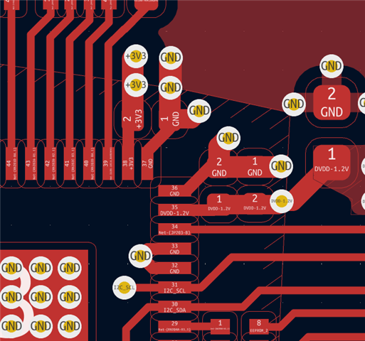
I get the first three pictures, but the forth one I'm abit unsure why you only want to remove one of the ground fill connections. Is this also ok?
Thanks for the last comments as well. I think I got it all sorted out:
I also really like these DSP chips! A real shame I cannot use sigma studio commercially.. I wish I could program my Fusion amps with sigma studio xD
Bonus question:
All these details regarding decoupling caps and so on. Do they really have a meaningfull diefference, or only something detectable with a scope at the right prope point?
I ask because when looking at commercial products such as this one (I know its a SHARC processor, but not the only one where I have seen it)
Its pretty obvious that anything called bypass/decoupling is just tossed to the other side of the PCB.
Backside
Front
Pictures from this thread: https://www.audiosciencereview.com/forum/index.php?threads/minidsp-2x4-hd-ddrc-24-v2-simple-measurement-and-teardown-pictures.50900/


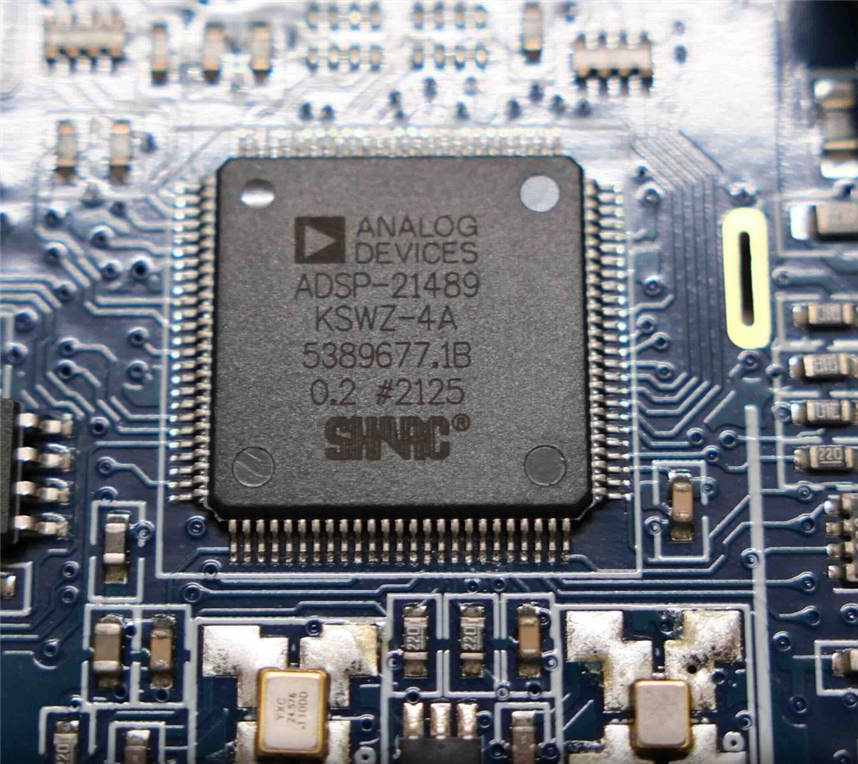
Hey Dave, happy new year!!
Did you have a chance to look at my last question?
Hello Danner,
Sorry, I have been very busy and distracted.
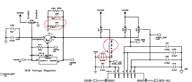
The item #3. Where I said caps on both sides of the ferrite bead. I was talking schematic wise not PCB sides.
Here is an example but not a great one. There are caps on both sides of the ferrite bead.
As far as the ground fill part of this discussion. Yes, I think you understood and did it right. It looks good. From the pin of the part you pass a bypass cap then hit the via to the plane then it gets to the fill on the top for the ground pins.
Some people do use SigmaStudio in somewhat of a commercial way. But, it is mostly companies who sell kits and small audio devices that are meant for hobbyists and they just show them a link to our web site and tell people to download SigmaStudio if they want to customize the product and they include the default schematic. It can turn into a hassle for us because you get a lot of people who are not electrical engineers trying to figure it out.
Most customers will program their own application that controls the DSP. One company actually has many different options for speakers, speaker drivers and crossovers and the installer chooses what is used and then their software will customize the EEPROM image. They are VERY much power users and were very good DSP engineers but still I had to help them a fair amount. They do super high-end home theaters and other film previewing rooms for Hollywood producers etc. Their audio performance standards are very high and they have been very happy with the SigmaDSPs.
On to your last bit of comments. The placement of the caps and the little things I have been talking about, like the placement of the caps and the vias, is a bit of an art and also a LOT of engineers are not aware of the issues. I have studied signal integrity theory but many others have not. Also, the SHARC folks have very few parts that have legs. Most of their parts are BGA style of packages and in that case it can be super difficult or impossible to follow these recommendations. It comes down to how the designers layout the pins. When we merged with Maxim we gained a bunch of new engineers and I have been impressed with them. Their BGA footprints almost always have the power and ground balls around the edges or where you can run them together and go out the side of the part. Then you can place the caps on the same side of the board. Some ground pins are only for references and not high currents so those are not as important.
What I have found is that often these details will make no difference until they do. Kind of like balancing something over the edge of a table. It will not fall off. Keep moving it out over the edge and it does not fall. Then once you pass the center of gravity BOOM! it makes a difference. The last move was small but made a big difference. I feel these PCB layout things are similar. They make little to no difference until you reach a tipping point and then it is a problem. Many of our eval board are not done well in my opinion but many were done before I joined ADI. Then there is the thing I mentioned which is trade-offs. You can never design a "perfect" eval board. You will have to compromise somewhere and hopefully it does not cause you problems later.
I have had several large automotive customers, well, the contractor who is doing the designs for the auto company, ran into issues with the amplifiers. They contact us and blame our chip. I come back and tell them the layout is the problem. After a lot of back and forth they make the changes and it solves the problem. So I have seen it make a difference and there are plenty of examples where it is not done well and the performance is fine! I think Mr Murphy may be involved in this and some Karma... So getting right with the spirit world will help as well! LOL.
I plan to make a video on this topic for my YouTube channel eventually. I have some ideas for demonstrations.
By the way, in the signal integrity classes it was all about the return current paths. The parasitic currents. Where do they go? This thinking helps a lot for layout of things like clock lines and data lines. That along with good bypassing will keep the power and ground planes much more quiet. It certainly is an art and I "visualize" a lot of this.
Dave T
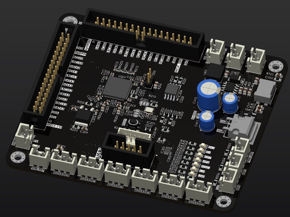
Hello Dave, I can imagine, but thanks for getting back anyway! Your comments have been a great help and I think I might be ready to try and get my board made. It's mostly just a test platform for future projects and an attempt to learn PCB design. Whenever I get this working with an input and output board I will start combining it all in one PCB for specific projects. This was just an attempt to experiment with individual parts without having to respin everything every time.. Hope it was a good decision :)
Okay I think the ferite beads should be okay then. What do you think of the other approach of having a seperate smaller LDO's for each named rail (IOVDD, AVDD and so on)? Bad, Better?
Well... Im one of those people.. It all started with a Wondom DSP board which does just that, links to you and now I'm here.. I'm no electrical engineer, I'm a mechanical engineer.. So Sorry about that But thanks for the example. Sounds like a great concpt they have!
Okay.. From mechanical engineering I'm used to a more black and white theory than this, but at least it explains why it is a topic with som many contradicting and confusing guides out there.. Thanks for clearing it up! Gotta be nice to Murphy and get some good karma built up then xD
Will be looking out for that video!
I have read a lot about the return currents of DC vs high speed digital and think I understand the concepts, it was mostly this decoupling stuff along with misleading information in the datasheets that I couldn't get my head around..
All that said.. I do think there is at least a 50% chance that this board may go smoking on the first power on xD
Thanks for your help!
Daniel
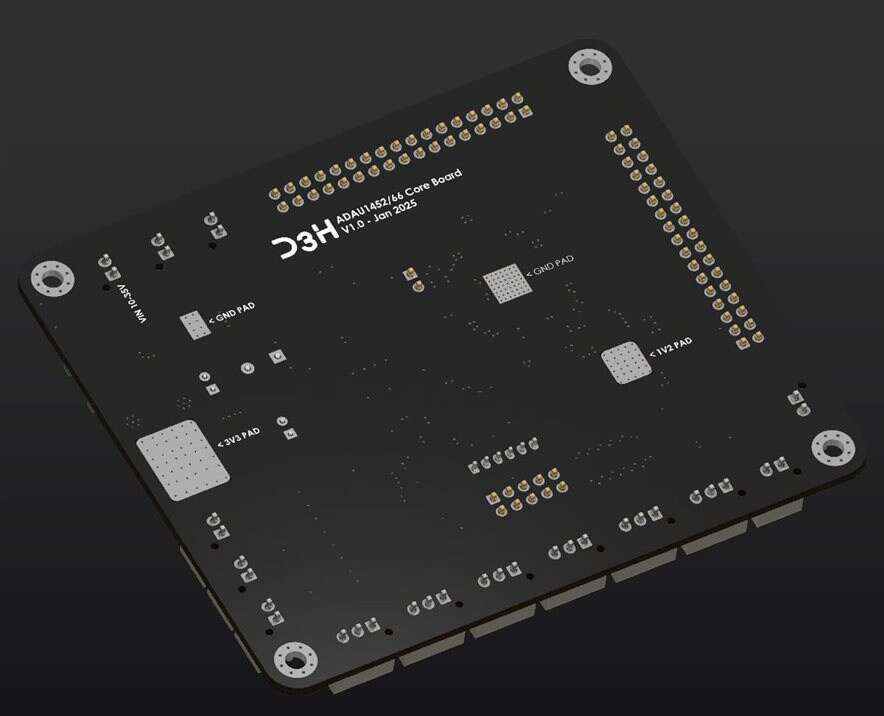
Hello Daniel,
Well, keep up the good work! You are a perfect example of why I treat all the people posting seriously because you never know where they will end up. You are learning a lot and it is only a matter of time before you are working for a company that will design and sell a high volume of units! Figuring out datasheets is another skill for sure! I have written quite a few now and see how it is done and it is difficult to include all the info and not leave anything out and add all the measurement conditions. It is almost an impossible task. Then add to it the pressures of release schedules and editors!
DannerD3H said:
I do think there is at least a 50% chance that this board may go smoking on the first power on xD
Gee, I have never had a board smoke or not work at first power up ... LOL, it is a rite of passage. If you have not done that you have not designed any boards. It is easier these days with all the design verifications you can do with the software but I still have had errors creep in despite all that! So cross your fingers and do not give yourself a hard time if there is a problem. Your board looks really nice.
You can probably tell I am also a professor so I am used to helping students gain confidence!
Dave T
Hi Dave,
Great discussion, but I have a question. You wrote:
> I do not like to see any pins tied to the EP that is under the part.
That's a new one to me for when the EP is stated as GND in the datasheet versus just an isolated slug.
Given on the PCB there's a piece of plane (so low R, low L) and has lots of vias to the ground plane (again low R and L since the vias are in parallel) connecting a pin to that on the PCB vs breaking the pin out with a piece of trace that's going to a single via - I would go for the thing with the lower R and L.
I assumed when the 1452 datasheet says the EP must be grounded it meant it's also connected internally to GND (some special bond wires or something?). But you're implying the EP is actually just floating? But if it's floating then there's no current and therefor no noise from it?
If it's electrically connected to the substrate with conductive adhesive there still shouldn't be any appreciable current under normal operating conditions? Going the other way, would current from a DGND pin that went to a via on the EP plane make that point noisier than the ground plane would already be if the GND pin was tied to a via connected to the GND plane few mm away?
1452 isn't really drawing gobs of power and/or seeing large, fast current swings when running, i.e. a few hundred mA at most? If this was some 10W+ FPGA or CPU that's drawing a couple of amps at a few GHz, then yeah, be very careful. But here, seems like a reasonably forgiving use case?
Please advise oh wise one :-)
Thanks,
Brewster
PS: Daniel, I have way more grey hair than Dave and I'm still learning...
Thanks for the confidence Dave ;)
I will let you know if it works or smokes! Will hopefully get it in end janurary :)
Brewster, if you stop learning then you must be bored :P
Hello Brewster.
This is best drawn out but I will try to explain it. Your analysis is spot on and correct. You mentioned that the PCB plane that the slug would be a soldered to it a good low impedance and low inductance path. Yes, indeed but here is what I have encountered and caused a serious issue with an automotive amp.
The analog and digital pins on a codec were connected to the EP and lots of vias (7 or so) to the ground plane. the pins were tied to the "EP" plane and also had some traces away from the part and eventually to other places on the top ground plane and other vias. But they were further away.
So the digital noise generated inside the part, (HF signals from the clock edges) would have a path to ground but the vias are inductive so there would be a voltage drop. This made this small plane ring with noise. It just happened that the analog sections of the part saw this path to ground as the lowest impedance and shared it. So now the analog section was picking up this digital noise. Well, the analog section of the part included the PLL so it would cause the PLL to lose lock or just not achieve a full lock. This small plane turned into its own small ground plane and a radiator and a shorter path than going to the actual plane.
Since the bypass caps were on the other side of the pins they might have well just not be there. They were not effective. So the idea is to force the current to both the power and ground planes to pass by the bypass caps on the way to the plane. This will make them the most effective and keep noise from getting onto the plane and keep any noise on the plane from getting into the part.
By the way, the troubleshooting of this issue all started because the TDM signal from the SHARC would jump from one BCLK delay to two BCLK delays! Intermittently! After a lot of work we found the PLL was not fully locked. So we switched focus and ruled out all the power supplies and other processors and anything else on the board.
Then we asked the company for a PDF of the PCB layout and it jumped out at me right away that they had the bypass caps on the bottom of the board and this small plane on the top. This codec did not have an EP.
So I asked them for a blank PCB. I soldered on just the codec and the bypass caps and applied external power and the PLL would not fully lock! They made my recommended changes to the PCB and they sent me a new one and Poof! locks quickly every time!
So the idea is to not have a shorter ground path between pins than if it were to go to the power plane. I suppose a small part with only one ground pin would not be an issue but those parts are rare.
Dave T
Hi Dave,
Thanks for the explanation. I can believe that, though part of me is thinking there was something else going on in that specific case. But can't argue with success...and I have battle scars from long ago trying to make stable low jitter PLLs out of discrete parts. One must invoke the dark arts sometimes :-)
One last question so I'm clear on it: The ADAU1452 PLL section ground is not tied to chip's DGND? Wouldn't that make a rather large loop for the return currents from the PLL output? Granted on chip it's like an very tiny current, but the electrons gotta go somewhere?
Brewster
Hello DaveThib
Just wanted to let you know that I got the boards and.. It actually works :O
I am still working on the DAC and ADC board. So for now I still just use the same chineese boards i used in my prototype. But all noise issues are gone. The signal is so clean that i cannot hear any difference when i turn the DSP on or off. That means that currently my amp is the limiting factor. Awesome!
I only found the following mistakes:
One silkscreen error on AUX ADC 0 - got the pins flipped
My MP7 LED works fine but i managed to connect MP6 LED to the input of the inverter and the signal from the DSP to the output because of a stupid Schematic symbol..
And my SMPS is noisy.. It makes an audible high pitch whine. Really a shame now that the signal is clean.. But hopefully it will be inaudible once the box is closed.
Any idea what may cause this? I know its a very weak question, its not even your chip.. The pitch varies with load. If i turn of parts of the ADAU chip the frequency of the pitch drops.
Thanks a lot for your assistance!
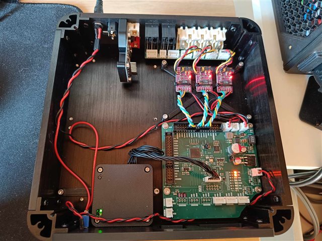
Hello DannerD3H,
Thanks for helping me feel better today. Because I thought I was the only one who will rev a board several times and still make some silly small mistakes!!!
It reminds me of my military electronics school. I did well and was top of the class through the course. I had a goal of getting 100 on the last theory exam. It was 100 questions!! I got a 99. The one question I missed was easy and everybody else in the class got it right! UGH! So I know the feeling.
But I am glad you got it going.
Regarding the power supply noise. It seems like it is varying the switching frequency as the load changes. This is not my area of expertise but I do know that when you deal with magnetics like transformers and inductors, as the current changes you can get a mechanical vibration or movement in the device from things like the core etc. The clue is that the pitch changes as you change the load. Others on the forum might have some suggestions. I suppose you could increase the load with just some large resistors but that is wasteful of energy and heat. It most likely not solve the noise just keep it from changing as you change things in the DSP. The current change would be small in comparison with the total current.
Another thing is just look at the way you have it mounted. If it is rigidly mounted to the chassis then it may be resonating the chassis and making it louder. If you do not need the heat sink of the chassis then try to use things like softer plastic standoffs or a rubber-like pad to keep the noise from coupling onto the chassis.
Dave T
Haha i think its close to impossible to avoid mistakes completely until you are at rev 10 xD
Thanks for the tips on the SMPS. I tried a big resistor hoping that the SMPS was running in burst mode or something. It didn't remove the noise but rather stabalized it as you say. So i guess the SMPS needs a redesign.. Or just use a big ass LDO xD
I've only had inductors make noise when driving "big" (several amps) of current. For a small switcher it strikes me as unusual. Have you looked at the switching waveform to see if it's what you expect? I would try a different inductor. As you noted if the load is light and the controller goes into pulse skipping mode you can end up with audible bursts. Maybe "downsize" the regulator if appropriate? A quick hack go down a (inductance/E6 ) value or two and see what happens. OTOH if the Isat of the inductor was low compared to the currents then that might have some unusual side effects but seems unlikely here.
YMMV
Okay.. so DaveThib you might still be able to help with my noise issue..
It turns out it has nothing to do with my SMPS. I designed the board in a way that I can bypass the SMPS entirely Cover My Ass (CMA) design. Supplying 5V from a bench supply changes nothing on the noise. When doing this test the SMPS is completely dead. I also had some help taking a quick look at the SMPS performance. It had a 200mV peak to peak ripple on the output so not the cleanest but I guess ok?. Also the switching frequence was rock solid at the 500kHZ it was supposed to but the PWM pulse lengths were wariyng a bit. For your info as well Brewster.
But to summarize, the SMPS has no effect on the whine I can hear. And it certainly isn't the source.
This had me scratching my head for a while.. Then I went lo tech and did this:
x10Yb7j941w?si=ix2MdQ4LxU2yFKv
So clearly somethings up with my DVDD generator?
Its these three capacitors that seem to be the culprits C208 mostly, followed by C211 and then C202.
This is the schemattic view:
They are all three Samsung, 10uF, 25V, X5R, 10%, 0805.
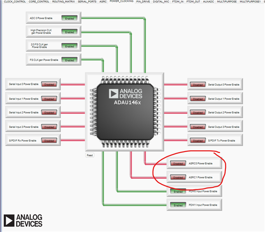
A side note. I can alter the pitch by changing some settings on the DSP thats power related. The frequency increases when I hipernate the DSP: jlDaQ2wiZWI
The freqency decreases when i start disabling some power sections: 9rqaGEcWGzc
Most noticably is the three outlined here. The remaining disabled ones also has some effect. The enebaled ones has no effect.
What did I mess up? Is it the mosfet? its a PBSS5330X,115 from Nexperia.
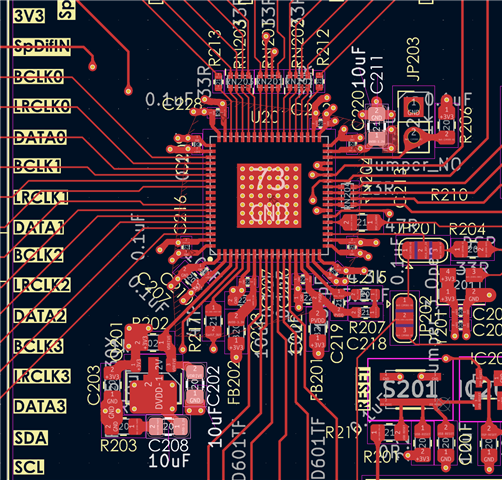
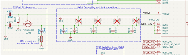
Now you really have me curious. I've done a few 1452 designs but never had something like that happen.
Dang, when I was writing about the inductor noise I almost added a "and you're sure it's not a cap" because that's not unheard (no pun intended) of. But it would have been the right question for the wrong reasons.
Vdrive should not have a cap on it.
Well maybe you never tried it because as you say that C202 is not supposed to be there.. Not sure why on earth I added that one. I think i got confused by this section in the datasheet with all those unmarked vias and then i just accidently added a third 10uF cap...
Can you confirm the following:
Remove C202 as its not supposed to be there
The vias shown on the image above are connected to the nets shown
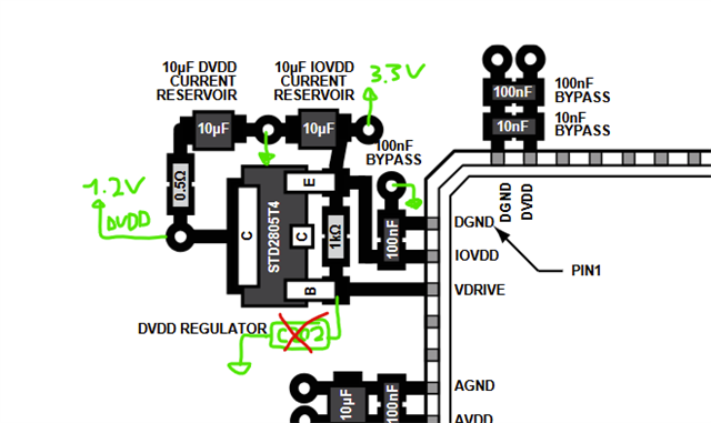
Removing C202 removed the whine!
I suspect with the cap there on the base your regulator could be more of an oscillator than a regulator.
Regardless mystery solved.
It sounded like an oscillator:P
Hello DannerD3H and Brewster,
Been a busy week for me. I started reading the recent thread and saw C202 and made a note, "remove C202" then kept reading and was pleased to see you all figured it out.
It obviously caused an instability with the internal regulator circuit. There is an internal OpAmp that drives the "Drive" pin so it must not like to drive that much capacitance and cause it to go unstable and oscillate. I have experienced this in other designs with discrete OpAmps where I was driving too much capacitance to create a rectifier for a metering circuit and the first OpAmp I chose absolutely did not like driving 1uf cap! So a 10uf certainly would cause an issue.
In that design I changed the OpAmp but also added a series resistor. When you look at the circuit if you place a large cap on the output, especially a ceramic one with low ESR. (In this case an old fashioned electrolytic might have behaved) With no series resistor you have effectively a dead short to ground for fairly low frequencies. This means there is no negative feedback for the OpAmp so the gain is huge!! You need the series resistor to isolate the filter and allow some feedback to the amp circuit. Good old analog design practices. I had to learn it again via the school of hard knocks! This was about 15 years ago now, pre ADI days for me.
Dave T
Yes everything is under control now
Please log in to reply.