How can I config the serial ports of ADAU1452 to use one BCLK and LRCLK to achieve I2S full-duplex communication?
I have an application requirement. I want to use a CODEC to connect ADAU1452, but the CODEC have only one BCLK and LRCLK, and SDATA IN , SDATA OUT.
I want to achieve I2S full-duplex communication.
I want to use ADAU1452 as the master devices,connect SDATA_IN0, and DSP generate BCLK and LRCLK, I also want to receive data from CODEC.
But what I find from "serial clock domain" in datasheet is "any serial data input can be clocked by any input clock", I don't know if "serial data output" can use input clock domain.
How can the clock and data sync ?
How can I config in "serial ports " in Sigma Studio?
Thread Notes
santha.vijay - Moved from Software and Development Tools to SigmaDSP Processors & SigmaStudio Dev. Tool. Post date updated from Wednesday, March 26, 2025 12:41 PM UTC to Thursday, March 27, 2025 4:57 AM UTC to reflect the move.
Audio Signal Processors
adau1452
software
SigmaDSP Audio Processors
Hello Yuchen001,
There are no connections between serial input and output domains, so you just have to externally connect (wire) the clocks between the input and output ports.
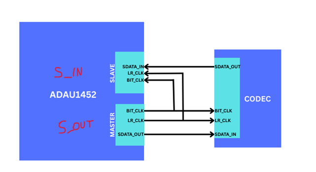
If you are using serial input port 0 to receive data from the CODEC and serial output port 0 to transmit data to the CODEC, then you can do something like this, you can take BCLK_OUT0 and LRCLK_OUT0, set it as master and split it ("Y'') and connect one pair of BCLK, LRCLK to the CODEC and another pair to the serial input port's BCLK_IN0 and LRCLK_IN0 pins respectively, make sure that you set the serial input port 0 as "slave from clock domain 0".
Please refer the block diagram shown below.
Please keep in mind that your MCLK_IN to the DSP and CODEC should be derived from the same master clock domain.
A common way will be using a crystal oscillator as the MCLK source to the DSP and using the 'CLKOUT' pin of the DSP as an input to the CODEC's MCLK source.
Feel free to reach out if you need more info on this.
Regards.
Harish
Hello Yuchen001,
I want to add a little to what Harish has talked about.
Harish is correct that the input and output click domains are separate. This is usually an issue when you have the Codec be the clock master. Then you MUST connect the LRCLK and BCLK to one of the set of clock inputs on the serial input ports AND to the serial output ports. Then set the data input to slave to the port pins you used.
In your particular case, you want the DSP to be the clock master for both the ADC and DAC sides of the codec. In that case then just use the internal clocks. Those are exactly the same because it is internally derived and then sent to both the serial input and output ports. So if I look at the drawing that Harish suppled, just set the Serial input port clock pins to be a master. You do not actually have to send it to the codec if the codec does not need it. By setting the port to be a clock master it will clock in the data and it has no idea that the pins are not connected to anything. The clocks going out of the serial output port will be exactly the same clocks so the codec will correctly send the data.
This is not a huge difference. It saves some external PCB traces but it does save a few nanoseconds for the timing of clocking in the data. Slave mode is the worst case for serial data timing.
Like I said, What Harish shows is perfectly fine. In your use case you could save a few traces.
Dave T
Please log in to reply.