Inquiry Regarding ADAU1401A Application (I2S Connections)
We are currently reviewing the implementation of the ADAU1401A in our project.
We have selected this part as it appears to offer the desired features at a cost-effective price point.
Our initial plan is to connect the ADAU1401A with our Application Processor (AP), peripheral devices, and a digital amplifier using the I2S interface.
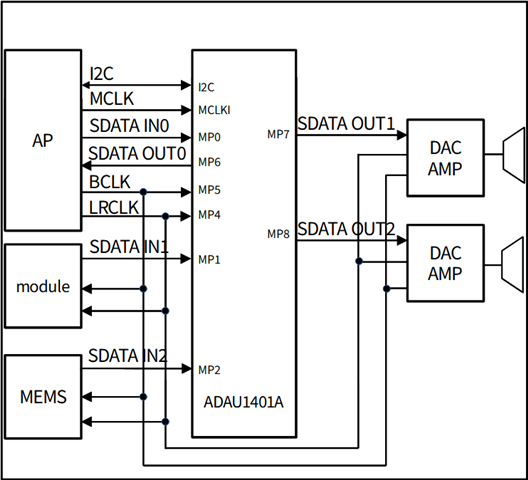
As we are new to audio implementations, we would appreciate it if you could review the attached connection diagram (specifically focusing on the BCLK, LRCLK, MCLK, input (IN), and output (OUT) connections) and confirm its feasibility for our intended application.
adau1401a
Audio Signal Processors
hardware
SigmaDSP Audio Processors
Hello NGH,
This looks pretty good. One thing I see missing is that you have to connect the LRCLK and BCLK to the MP4, MP5 and also to MP10 and MP11.
You are sending those clocks to a lot of places so you might want to consider using a clock distribution/buffer IC to isolate and drive all those parts. You can design the board so there are jumpers around the buffer and in your initial testing experiment with it and without it and see if it is needed. It might save headaches later with flaky problems and clicks and pops due to poor signal integrity on the clocks.
It looks like you are planning to use regular I2S rather than TDM which is always a good idea because it keeps the bit clock frequency lower.
But it looks good. Just make sure the LRCLK and BCLK are properly divided down from the MCLK. You are providing all of these from the Applications Processor so that should be simple to do.
Dave T
Hi Dave Thib,
Thank you for your feedback.
I understood that LRCLK and BCLK on MP10 and MP11 are pins used when the ADAU1401A is the master. Is it okay to connect them to MP4 and MP5 as well?
Hello NGH,
Let me chime in here for Dave since he is in different time zone.
What he meant is, since you are sending a single clock source (from AP) to all modules (including AMP), you will have to set the serial output port to be a slave and send them the same clocks. In simple terms, you should connect your LRCLK, BCLK from AP to MP4, MP5 (input port always slave) and to MP10, MP11 (output port optionally slave), so every part will be running on a same clock.
NGH said:
I understood that LRCLK and BCLK on MP10 and MP11 are pins used when the ADAU1401A is the master
When the serial output port is master, MP10 and MP11 will be outputs (will generate its own clocks and send them out along with data), when serial out port is set as slave, MP10 and MP11 will be inputs, so you should provide a clock so that it will output the data.
In your case, you will have to set it as slave, thus you should provide the same synchronous clock from AP to MP10 and MP11.
Below is your updated block diagram.
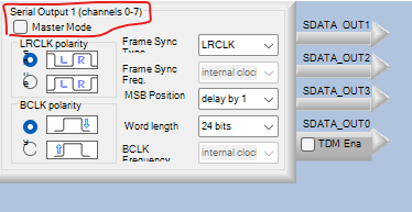
To run the serial output port as slave, you have to let the box to be unchecked (default setting)
As Dave said, since you are sending your clocks to a lot of places, make sure your signal integrity is maintained otherwise you will have to use a clock buffer.
DaveThib said:
You can design the board so there are jumpers around the buffer and in your initial testing experiment with it and without it and see if it is needed. It might save headaches later with flaky problems and clicks and pops due to poor signal integrity on the clocks.
You can try what Dave suggested above.
Hope this helps!
Regards,
Harish

Please log in to reply.