TDM4 ASRC problem
Hello, here I am again
using FPGA to merge 2 i2s to TDM4 as described on page 57 of the 1467 datasheet.
test-1467-16ch_All_rates.dspproj
but no output at all, anything wrong?
Best regards,
Pan
Edit Notes
missing one tdm2
[edited by: PowerPan at 2:07 AM (GMT -4) on 5 Jun 2025]
Audio Signal Processors
software
adau1467
SigmaDSP Audio Processors
Hello Pan,
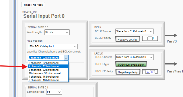
Technically, it is actually TDM4 so you need to set it to pick up four channels.
Do this on all four serial ports and I think you will be fine. The ASRC settings seem correct.
I am surprised that you got nothing. I would of expected that you got at least half the channels.
Check that the clocks are correct going into the clock pins for serial port zero. You should have a 50/50 duty cycle LRCLK at 48kHz. Then the bit clock needs to be 48k * 32 * 4 = 6.144MHz.
This bit clock frequency is not super high but you will still need to have short jumpers and I would run a ground wire along side the jumper or twisted with it for a return current path. If your signal integrity is really bad or levels are low then you will get nothing or get garbage.
I just ran across that in our lab last week. A 12MHz bit clock did not work well enough with the standard meter long coax cables that the Audio Precision uses for the serial port. We had to switch to the short twisted pair cables that you can get from AP. But the level was low and we were getting garbage. Full scale garbage!
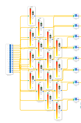
I also glanced at your project to see what you are doing. I like that you did place some meters fairly early in the signal path! Yes! Well done! Great troubleshooting practice. You could also move them before the mixer but the chances that you are sending the same exact signal out of polarity so they fully cancel and get nothing is rather slim.
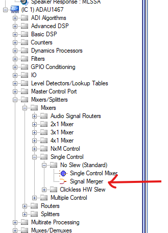
Also, the mixers use a few more instructions because you can add gain. This might be in your plans but if I am making mono or just mixing two things together I will usually use either a simple addition block or the Signal Merger where it also reduces the summed level by 6dB. This is not a huge deal and you may want the flexibility to adjust the individual levels of each input. Should you find that you are running out of MIPS this might be a place to gain back a few.
Send some scope screenshots of the FPGA outputs if it still does not work. Take these as close to the DSP as you can so you can see the signal level and integrity.
Take a few and make them look like these in my old post:
(+) How to Take Meaningful Screenshots of I2S Audio Signals - Q&A - Audio - EngineerZone
Dave T
Hello Dave
I do get 0-7 ch work, but I could only connect to low 8 ch or high 8 ch to test independently. All the clocks are feeding in the right way by a clock distributor. A good suggestion for the mixer. I used to use what you told on 1452, but I couldn't find the mixer without a search function. For just testing, and since the part I chose worked, I will do it later.
I'll try to fixed the problem today, or I'll upload the chipscope output of the FPGA capture here. (I did not leave the test point on the board)
Best regards
Pan
Hello Pan,
Yes, we try to hide this stuff so nobody can find it! Saving it for a rainy day I guess? (OK enough of the poor humor this morning. )
Here is where you find the signal merger:
The basic signal add without any gain compensation is under the Basic DSP, then Arithmetic Operations and it is called Signal Add.
Gee, I find it interesting that you are getting 0-7 and not 8-15?... I would have expected that you would get channels 0, 2, 4, 6, 8 ,10, 12, 14
All the even channels since you had it set to 2-channels but are feeding it a four channel TDM signal.
Verify that the bit clock rate is what I mentioned in my last post.
Then look at the signal on the screen. You really should have to change the serial port settings to be four channels.
Dave T
Hello Dave
thanks for the hint. I got and replaced the component.
and I could tell that if all channels were mounted, only half were in working status by the signal monitor.
there is a bug for the FPGA output channel 4 didn't come up, maybe the timing issue and the FPGA merge is working but not all ASRC could output at the same time. I'll modify the schematic by putting 8 more signal indicators and will upload the result.
let me explain more about the chipscope snapshot above, FPGA will output the word clock to RME sound card for better clock control but needs to sync the output from the SPDIF receiver and send it to DSP with a unique clock from channel 0, because the SDATA_IO couldn't meet the IO requirement, so the FPGA had to merge 2 I2S into TDM4 and send to DSP. so in above picture, datIn0 comes directly from SPDIF receiver, and RXin0 is the sync data with wckREF, will delay 2 WCK and then output, then dspIn0 is the TDM4 data merge with RXin0+RXin4. but unfortunately, RXin4 did not come out with the expected result. just ignore this but, all other TDM4 works fine.
Best regards,
Pan

Hello Dave
After I kill the bug in the FPGA, all channels work fine. Some constraints in the FPGA cause the error. but I wonder why so slow speed can cause the bug.
Best regards,
Pan
Hello Pan,
I am not sure what exactly was at slow speed? If it is a bit clock then what will happen is that not all of the bits will be clocked in when the frame ends.
The LRCLK is in control. It starts the frame and ends it. The register settings setup the structure of the big long shift register to figure out how it is divided and where the data will be once the data it clocked into the shift register. This is all done with fancy gating and logic in the DSP hardware. But, it is dumb. You set it up and it assumes that the data was correctly clocked in.
So the LRCLK starts the frame and the bit clock starts reading in the bits and shifting it down the shift register. When the end of the frame hits (LRCLK) then what ever is in the shift register is transferred to the memory location with a parallel data move. It has no idea if there were enough bit clocks to properly read in and place the data in this shift register. So if the bit clock frequency is wrong the data is in the wrong place and you get strange results.
Some of our parts will actually count the bit clock transitions and if it is wrong it will mute the audio. Our AD1938/1939 codec does that. So does the ADAU1701 DSP. This DSP you are using is so much more flexible and does not have converters so it does not mute anything. It is up to you to feed it the proper clocks to properly clock in the data.
I am glad you got it working!!!
Thanks,
Dave T
Hello Dave
that's the timing constraint for the FPGA, cause so many FIFOs in the design, need to optimize the floorplan carefully or it will not meet the timing requirement, then comes the bug. that's why I don't care if the SDATA_IO pins work or not cause I could easily walk around that but, if I could do less job to make it work, of course I'll choose an easier way to implement it.
My design will include many programmable parts to meet my requirement of softwiring the hardware, so my design will be highly flexible. and since I'm a software guy, most hardware teams could hardly understand what I needed, so I had to do it myself.
Best regards,
Pan
Please log in to reply.