Request for Review of Audio Speaker Architecture Using ADAU1401
Dear Analog Devices Support Team,
I would like to ask for your support to review the audio speaker architecture of our design and confirm whether the proposed concept is technically sound.
System overview:
Host processor: Rockchip CM3588
DSP: ADAU1401
Power amplifiers:
4 × TAS2780
1 × TAS6421-Q1 (TAS6421QDKQRQ1)
Proposed audio architecture:
The CM3588 outputs digital audio via I²S.
The I²S interface is connected to the ADAU1401 for audio processing (EQ, mixing, volume control, etc.).
The I²S output of the ADAU1401 is then routed to five digital-input power amplifiers (4 × TAS2780 and 1 × TAS6421-Q1).
The amplifiers share the same BCLK / LRCLK / MCLK, while audio data is distributed accordingly (separate data lines or TDM, depending on configuration).
I²C is used only for control and configuration.
Questions we would like to confirm:
Is it valid to use ADAU1401 as an I²S audio interface between CM3588 and multiple digital-input amplifiers?
Are there any limitations or concerns when routing the ADAU1401 I²S output to multiple amplifiers in parallel (clock loading, signal integrity, drive strength, timing, etc.)?
Are there any recommended constraints (maximum number of I²S loads, need for buffers, series resistors, or clock distribution best practices)?
From an Analog Devices perspective, is ADAU1401 suitable for this type of digital audio distribution, or would you recommend a different ADI DSP/codec device for this architecture?
We would appreciate your feedback before finalizing the schematic design.
Thank you very much for your support.
Best regards,
Phong
Audio Signal Processors
tas2780
hardware
adau1401
tas6421
SigmaDSP Audio Processors
Show More
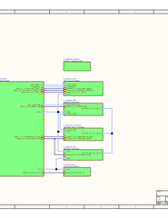
Hello Phong,
First I want to clarify some terminology that you are mixing up which makes it confusing. I2S is a STEREO format and very specific of 64 bits per frame and a delay of one BCLK for the data and the data is 32 bit but you can send 24 or 16bits by left justifying the data so sign bit is in the correct location.
TDM is for multiple channels and lots of different configurations. TDM-2 is possible with many configurations. It seems like you are thinking of TDM-8 but I have no idea of the number of bits per channel you intend to use?
So your labels I2S_DATA_TDM are confusing? Is it I2S or TDM? But, you have explained enough that I think I understand what you are wanting to do however, there is one confusing thing. You mentioned two channels going into the DSP yet I see two I2S lines in your schematic? So four channels?
You are going into Input 1 and Input 2 and not using Input 0 so these four channels will appear in the DSP as channels 3,4, and 5,6. Channels 1 & 2 will have no data because you are using that pin as GPIO
This is one of our older parts and this was early in the history of the industry using these serial standards but you should be able to do what you need for this application.
One other thing is that you mentioned drive strength. This part again was designed a long time ago so there are no registers for adjusting drive strengths. You have series resistors in your design which is great and might prove to be handy if the drive strength it too much and you have too much overshoot.
There are no sample rate converters in this part so it is good that you are distributing the same MCLK to all the chips. This is very important. Good job with that!
Any newer chips with more flexibility of the serial ports and the pin drive settings will be a lot more expensive for you and take up more PCB area. If you have high volume needs and a little time before product release then contact me directly. I looked up your company name and you used a GMAIL and no company name in your profile.
It is good to leave the DAC outputs open but the ADC inputs are better to be tied to the CM voltage and have a cap to filter out noise. There is a cap on the CM pin so you are good there. Just tie the unused ADC input pins to CM. Having a 0R resistor is a good idea should you change your mind later.
I cannot comment about the power amps. You know we have some good amps in our portfolio.
So should you think about needing more DSP processing and more flexibility then look to the ADAU1452 family of parts. Since you are not using the codec features of this part that makes it easier to switch. So I will slightly change what I said above because you are not using the codec built into this DSP. Only the DSP. So the ADAU1452 is only a DSP.
Enough for now....
I hope this helps.
Dave T
Dear Dave,
My name is Phong, and I am from E-Life Technology, Vietnam.
I see that the ADAU1450 and ADAU1452 datasheets are quite similar, and the ADAU1450 is much cheaper.
Can I use the ADAU1450 instead?
When connecting the CM3588 to the ADAU1450, should I use the I²S input pins?
And when connecting the ADAU1450 to the power amplifier IC, should I use the I²S output pins?
Could you please describe how the pin connections should be made?
Thank you very much for your support.
Best regards,
Phong
Hello Phong,
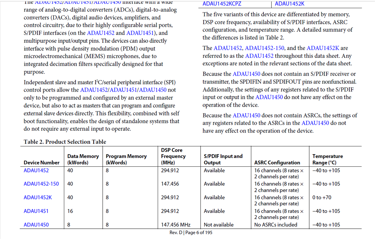
Yes, the datasheets are the same exact datasheet. The differences on the devices is detailed on page 6:
Phong said:
When connecting the CM3588 to the ADAU1450, should I use the I²S input pins?
And when connecting the ADAU1450 to the power amplifier IC, should I use the I²S output pins?
Yes, and Yes.
Dave T
Dear Dave,
1. With this architecture, should I use standard I²S (not support TDM) or I²S (support TDM) on the CM3588 to connect to the I²S input of the ADAU1451?
System overview:
Host processor: Rockchip CM3588
DSP: ADAU1451
Power amplifiers:
4 × TAS2780
1 × TAS6421-Q1 (TAS6421QDKQRQ1)
Proposed audio architecture:
The CM3588 outputs digital audio via I²S.
The I²S interface is connected to the ADAU1451 for audio processing (EQ, mixing, volume control, etc.).
The I²S output of the ADAU1451 is then routed to five digital-input power amplifiers (4 × TAS2780 and 1 × TAS6421-Q1).
I²C is used only for control and configuration.
2. Additionally, I would appreciate your recommendation regarding the I²S output configuration from the ADAU1451.
Should I connect all five amplifier ICs to a single I²S output port of the ADAU1451 (sharing BCLK/LRCLK/DATA), or is it preferable to distribute them across multiple I²S output ports, for example:
One dedicated port for the TAS6421-Q1
Two separate ports, each connected to one TAS2780
The remaining two TAS2780 sharing one port
From a signal integrity, synchronization, and overall system stability perspective, which architecture would you recommend?
Thank you very much for your guidance.
Best regards,
Phong
Hello Phong,
You are asking good questions but there are so many variables that I do not know that would affect the response.
Like connecting all the LRCLK and BCLK outputs of the serial port. Five is a large fanout so that is not great but still could be possible if the parts were very close together and the PCB layout was well done. If you are not using the clock pins on the other serial ports for GPIO, then yes, it would be best to use all of them to send to the amps. One port will go to two parts but for the other three ports just send it to one amp.
You can set the serial ports to send the same clocks from the same internal source. Then you have more flexibility to have different drive strengths for each pin.
I do not know anything about the CM3588 so I cannot help there. If that module is running on the same MCLK then you may be able to not have to use an ASRC. If it does not output I2S clocks that are derived from the same MCLK then you will need to use the ASRC on those input signals.
We have a lot of great digital power amps. You should look into it.
Dave T
Dear Dave,
I would like to clarify one more point regarding the serial audio interface between the processor and the ADAU1451.
For the connection between a generic processor and the ADAU1451, is TDM support required on the processor side, or is standard stereo I²S sufficient?
If the processor only needs to transmit two audio channels to the ADAU1451, can standard I²S mode be used without any limitation? Under what conditions would TDM mode be necessary for this interface?
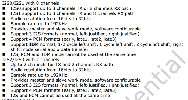
I2S0 and I2S1 support TDM mode.
I2S2 and I2S3 do not support TDM.
My understanding is that the processor-to-DSP connection does not require TDM support, and standard stereo I2S is sufficient.
This is because the I2S outputs of the ADAU1451 (which support TDM) are used to connect to the power amplifiers.
Hello Phong,
The serial input ports and the serial output ports are very much separate and can operate in whatever mode you choose. With clocks of your choice.
Then within either the set of serial input ports or the set of serial output ports, those ports also can function independently if desired.
Depending on your system requirements. You can input up to four I2S signals into the DSP. This would be eight channels of data, two per serial port. You can even clock them from one set of clocks!! Either all from an internal clock and only use one serial input port to send out clocks to the source device, or you can receive clocks from a source device and internally, clock up to all four of the serial input ports without having to "Y" the pins externally. It also frees up some of the MPx pins for use as GPIO.
So yes, you can bring in up to eight channels of I2S data, two per data line, into the DSP. But, that would use up all of the serial input ports so no other signals can be brought in.
Dave T
Dear Dave,
Yes, I understand. Thank you for your supports.
Best regards,
Phong
Please log in to reply.