ADAU1701 /1401 Recommended Crystal Layout
Dear Analog,
We have designed a system using the ADAU1701 and have experienced inconsistent communication to the unit over I2C and SPI. We have narrowed it down to the crystal oscillator being at fault.
It appears to be an identical issue to a previous post. https://ez.analog.com/thread/9384#33074
When we remove the 100R damping resistor the communications works.
Can Anolog please comment on our findings based on our layout below.
Is there an obvious flaw in our crystal circuit layout?
Is there a recommended PCB layout for the crystal, load capacitors and damping resistor?
Should the damping resistor value be changed?
We are following the recommendation on page 18 of the manual,
Fundamental Crystal, 18pF. (Abracon ABLS-12.288MHZ-B4-T). 22pF load capacitor and 100R damping resistor.
https://www.analog.com/media/en/technical-documentation/data-sheets/ADAU1701.pdf
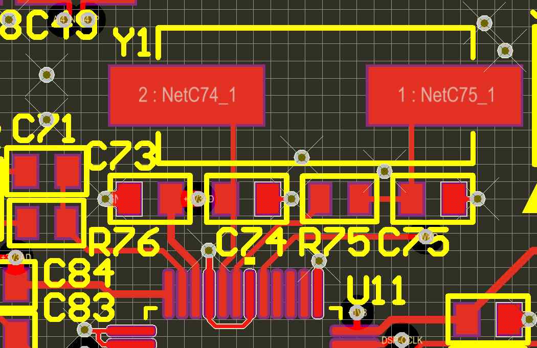
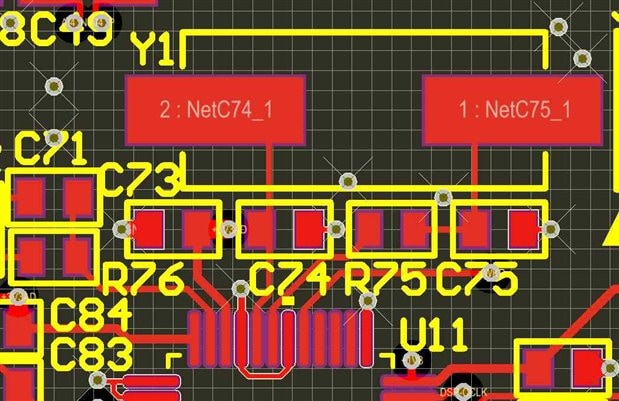
Our layout is shown below. It is a 4 layer stack with a ground plane directly under the DSP and crystal. There is no copper pour on the top layer
Audio Signal Processors
crystal
SigmaDSP Audio Processors
layout
adau1701
Hello euanbrown,
I don't see an issue with the layout of the crystal circuit and its associated components. I do see an issue with the PVDD power and ground pins and the Loop Filter (LF) pin. This could be causing the PLL to take too long to lock. The power pin bypass caps can also cause issues with too much noise on the ground which can cause issues as well. By reducing the damping resistor you are getting over this noise. That is my guess based on the information you supplied.
1) Loop Filter:
This needs to be returned to the PVDD pin without going through vias and through a power plane. By going through vias and to the plane to return back to the PVDD pin you are adding inductance to the circuit and then also adding in the noise on the plane.
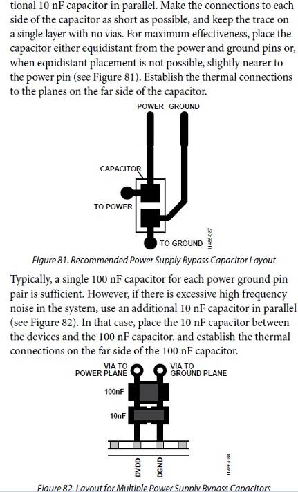
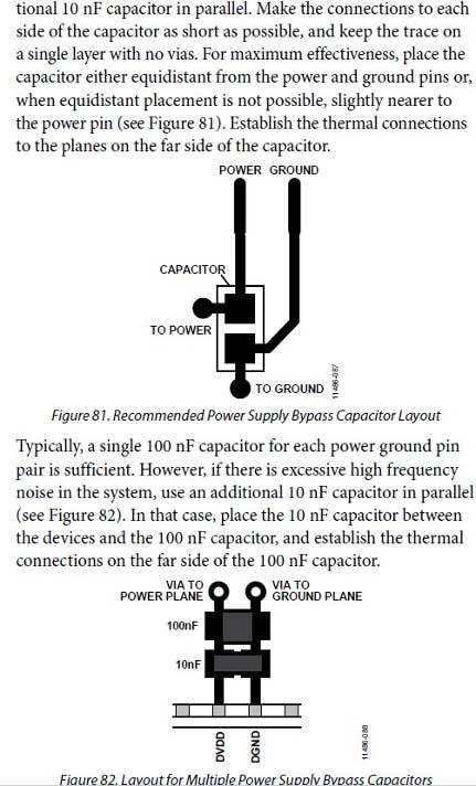
2) All the power bypass caps in your entire design, including other parts, need to be close to the pins and not use vias to return to the ground pin. This will help make the caps more effective. This will help keep any noise generated inside the part from actually getting out onto the power plane. It will also help any noise that is on the power or ground plane from getting into the part. So it works both ways. By doing all your bypass caps like this you keep the noise down on the planes.
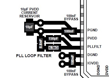
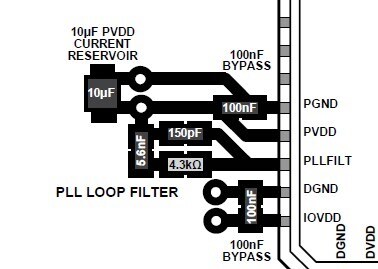
The ADAU1452 datasheet has a good applications section describing how this should be done. I will paste in part of it here.
What could be happening is that the PLL is taking too long to lock and without the PLL locked you cannot communicate with the part.
At this point I don't think the resistor value needs to be changed. Try the other layout changes first.
Thanks,
Dave T
Thank you Dave for your fast response.
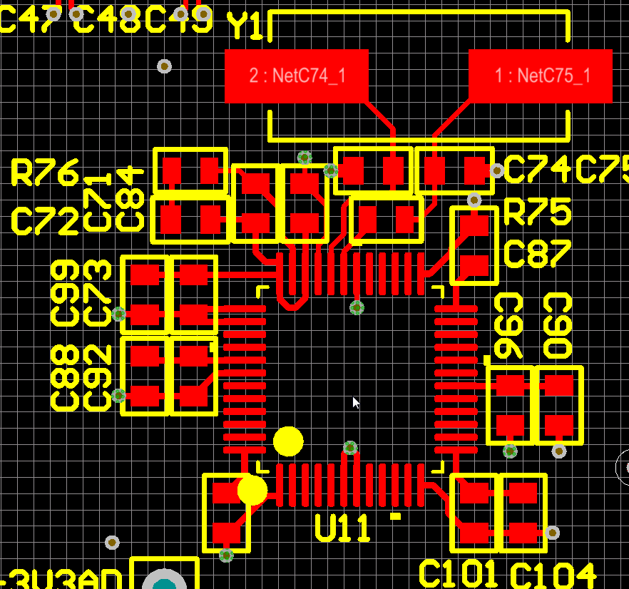
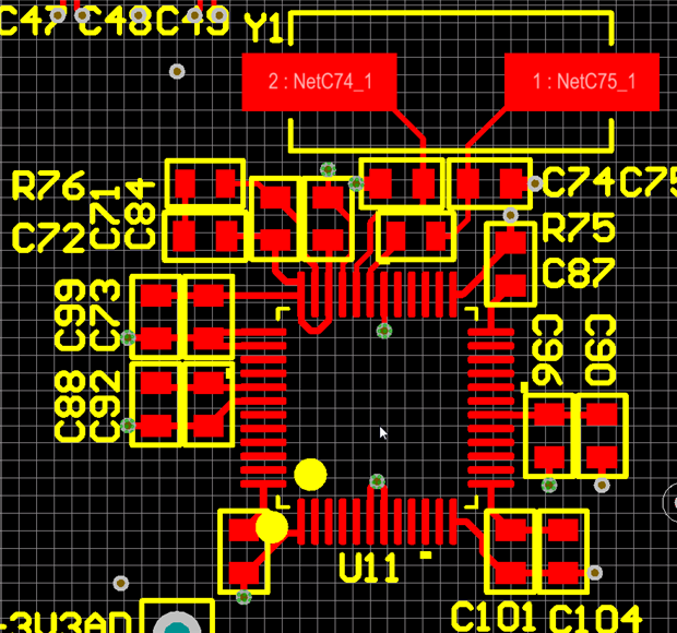
I have modified the layout to fit all the critical decoupling and crystal components as per your suggestion.(rest of circuit still to be completed)
Can you please confirm the layout below looks suitable
Hello euanbrown,
Yes, that looks good. We really needed to have a ground pin next to the IOVDD pin, pin 18, but we did not. I was not part of the design team so there may have been a reason for it.
Anyhow, I think this should help. Let me know.
Dave T
Thank you Dave,
We will manufacture the new design and I will report back our findings before closing this discussion.
Hi David
You have commented on the partial layout provided by Euan.
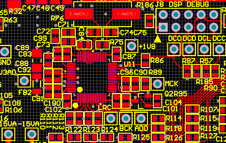
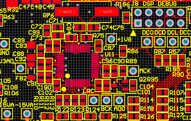
Would you mind to review the layout below, now with all connections routed.
Regards,
Les
Hello Les,
I did notice something. The PLL Loop filter needs to return to the PVDD pin. Yes, ultimately the AVDD pin and the PVDD pins are powered off of the same power source but it is important that the return current path is short on the PLL loop filter so that is why we placed the PVDD pin right next to the PLL_LF pin.
I think there is room in your design to turn the loop filter around a bit to be able to connect the loop filter between the PLL_LF pin and the PVDD pin.
Otherwise, you did a great job with the rest of the bypass pins.
Dave T
Hi David,
Thank you for reviewing the layout and your comments.
I re-arranged the PLL loop filter connections as you suggested.
The ADAU1701 data sheet states:
Based on this I thought that minimising the length of the PLL_LF (pin 35) trace was of higher priority. But, yes you were clear on this in your previous comments.
Related question.
Would you see any advantage of placing a copper fill on the board top layer directly under the DSP chip, connected with vias to the ground plane?
The board is a 4-layer board and the ground plane is located directly below the top layer. On the next layer the chip power connections are routed with the analog signal traces placed on the bottom layer.
Regards,
Les
Hello Les,
It looks like the person who originally wrote the datasheet made an error by not showing the loop filter running back to the PVDD pin. I have spoken with the designers of this part, and several other parts, many times about this subject and they all say it must return back to the PVDD pin because that is the connection to power for the PLL and the filter's return currents must return to the source which is the PLL power connection. If it is a long return path then there is a greater chance for noise to interfere with the PLL feedback loop.
On the ADAU1452 we show an example layout and also mention that the filter needs to return to a specific pin. Here is a screenshot from that datasheet.
Regarding placing a ground fill directly under the part. No, there is no advantage that I am aware of. If you do put in a copper fill then I would recommend that under the part be an isolated square with several vias to the ground plane. Do not tie this fill to any of the ground pins of the part. I have seen this fill become a small ground plane separate from the main ground plane by several inductive vias so it will become a path for noise between the analog ground pins and the digital ground pins with no bypass caps. Sort of like its own little ground plane that is not properly bypassed. It can also become a radiator or EMI. So if you do place a fill just isolate it from the pins of the part.
Dave T
Hi David,
Thanks for your explanations.
I either couldn’t see any advantage of the top layer copper fill under the ADAU1701.
Regards,
Les
Please log in to reply.