ADAU1701 ADC noise - even with new design
Hello everyone,
I have some problems with noise from the ADCs at my ADAU1701.
We started making products (e.g. active speakers) with this DSP several years ago, but we always had problems with input noise. With adjusting the input and output levels we managed to make this acceptable, but now we want wo make a new product line and of course we want to improve this.
Because we make most of our electronics in THT we designed a small PCB, containing most of the necessary peripherals. It is a 4-layer PCB and in the past we even used THT-parts on it, except the adau of course. Because I thought, the subotimal layout and dimensions of the parts would be responsible for the noise, I designed a pin-compatible full-SMD-version of it and tried to fulfil all the requirements concerning the layout. We got 4 samples of the PCB now and the noise is still the same.
Some things about my design:
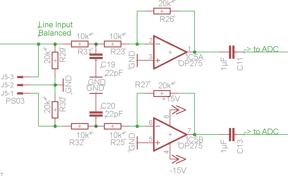
For the input of the system we always use an additional buffer stage, shown below.
This one does definately not produce the noise I am talking about, If I just cut the connection between this and the input-ADCs there is no change.
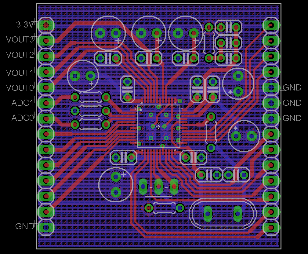
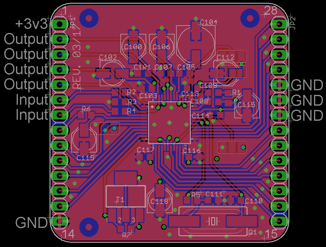
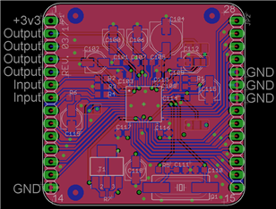
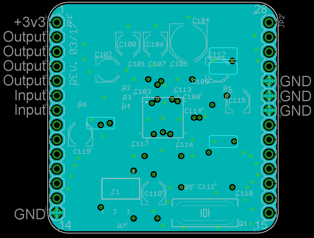
The ADC-resistors are 18kOhms and they are all on the DSP-PCB. Here is the layout of the old and the new version:
And the inner layers:
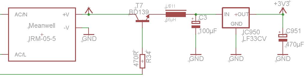
Power Supply:
Other things about the project:
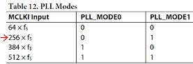
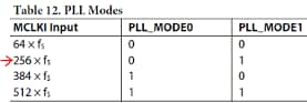
The DSP is running at 96kHz with a 12.288MHz crystal, PLL Mode
We use the Input-ADCs as balanced input in this project and as stereo-input in others with the same noise problem
I made a simle program with an adjustable volume block between inputs and output to verify that the noise is coming from the ADCs
What I already tried:
replace the resistor in the PLL by a capacitor, like seen here in this board somewhere, no effect
replace with other values and even disconnect the resistors on the ADCs, no effect or worse noise
make a completely new layout (see above)
put an inductor in the 3v3-supply, right in front of the DSP-PCB, no effect
Add a small offset to the ADCs, like seen here in this board somewhere, no effect
mute or power down the ADCs, -> silence, of course
Now, I do not have any ideas anymore, what I can try. From the evaluation boards (we have the old, large one and the mini-version) I know that the noise does not need to be this much.
If anyone has some ideas about that, it would be very helpful. We want to start the production of the new product line very soon and I want to fix this issue.
Thanks in advance,
Hanno
Audio Signal Processors
SigmaDSP Audio Processors
adau1701
Hello Hanno,
In your post you mention this:
This one does definately not produce the noise I am talking about, If I just cut the connection between this and the input-ADCs there is no change.
Can you explain this more. I am not sure which one "this one" was. There is a version that does not have the noise?
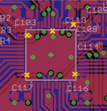
Thanks for providing the layout. Both layouts are not grounding the bypass caps properly which will make them less effective.
Do not connect the ground pins directly to the ground plane. Have them run to the bypass caps first then go to the ground plane. The thru hole version on the left you should just remove the vias and run the traces to the caps. I am assuming the thru-hole caps are connected to the ground plane.
The SMT version is a little trickier. Do not attach the ground pins directly to the ground plane. Have them go via a trace to the caps then to a via to ground. Tying them all to one ground fill on the top layer will create a small plane that will have a lot of noise on it and this is where every pin on the part will reference to. So have the power pins go to the bypass caps only. Then to the planes.
Read this post from last week:
https://ez.analog.com/message/299867?commentID=299867&et=watches.email.thread#comment-299867
Thanks,
Dave T
Dear Dave,
first of all many thanks for your reply! I think I see the point.
This one
meant the input buffer stage on the main PCB.
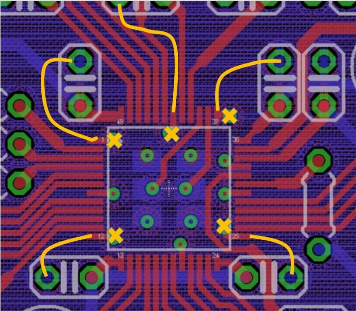
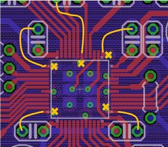
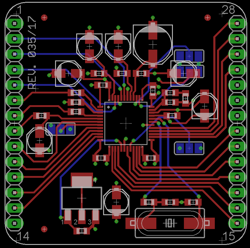
I understood what you mean about the supply-pins. So what I can do is just remove the top-GND-plane and even that one on the bottom and just use one of the inner layers as GND-plane and the other one for the 3v3, correct? I also rearranged the capacitors such that each supply-Pin is close to the capacitor and the corresponding GND-pin has a few mm distance from the capacitor, before it reaches is and then it is lead through a via to the GND-Plane.
After the changes, my layout would look like this:
Do you think this will have better performance?
Thank you and best regards,
Hanno
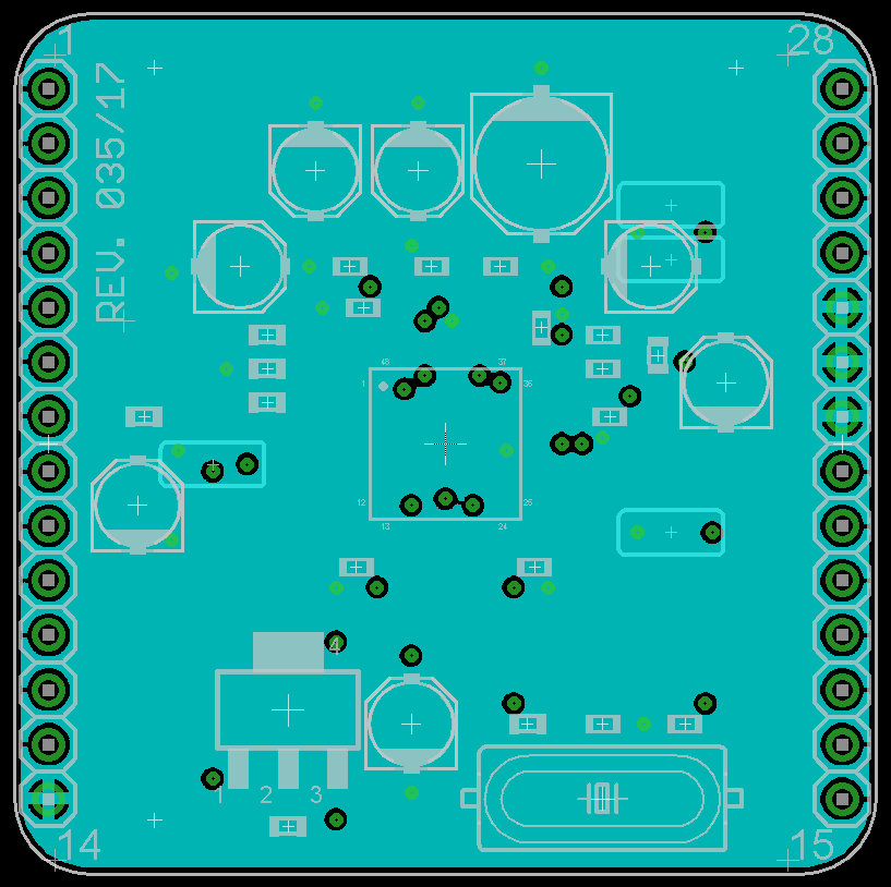
Hello Hanno,
Pin 42 needs to go up to the cap that is bypassing the FILTD pin.
Pin 47 also should bypass directly to pin 1. This is a little bit more tricky. I think you can run the ground around the AVDD bypass cap to the FILTA bypass cap. The large electrolytic bulk cap going to AVDD does not have to have a direct connection. It can be tied to the power plane and so with that trace removed you can get ground up to the FILTA bypass cap. I think I described this properly. I don't have time to draw something up right now.
Regarding the ground planes on the top and bottom. Those are fine, you can fill in ground. I am not certain of the overall benefit of doing this. On the positive side it will help to prevent crosstalk and coupling of signals. On the negative side it does add some more stray capacitance. I think they are a good idea. The only two things to look out for is to not tie directly to the ground pins of ICs (It is OK for pins that only need to be tied low but are not ground pins) Then the second thing is to make sure the copper fill is actually grounded and not floating. Small islands of ungrounded copper is really bad and can cause crosstalk.
If you do a top fill then under the parts make sure there are plenty of vias to the ground plane and do not tie to the part ground pins. For parts that have an EP under the part that needs to be grounded you must use plenty of vias (7x7 or more depending on the size of the EP) and do not tie to the part ground pins.
This should help the performance. Bypassing in this manner will keep the part from dumping noise onto the ground plane. Then parts like the input buffer will not be referencing to a noisy plane.
Let us know how it goes. There are always several factors and I do not know your entire system very well. What I described here is a starting point.
In looking at your power supply I would also place some 0.1uf ceramics along with the 100uf and 470uf caps on either side of the regulator. I do not know what the regulator datasheet says about bypassing so read that datasheet but it seems to me that it would be a good idea.
Thanks,
Dave T
Dear Dave,
thanks again for your input.
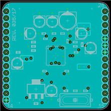
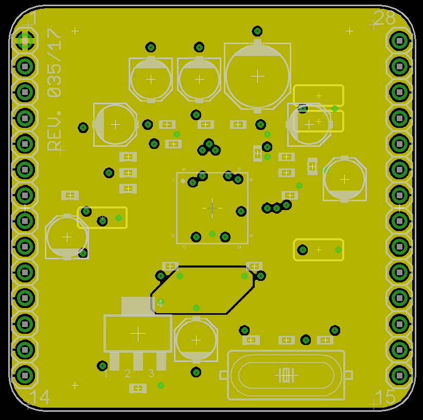
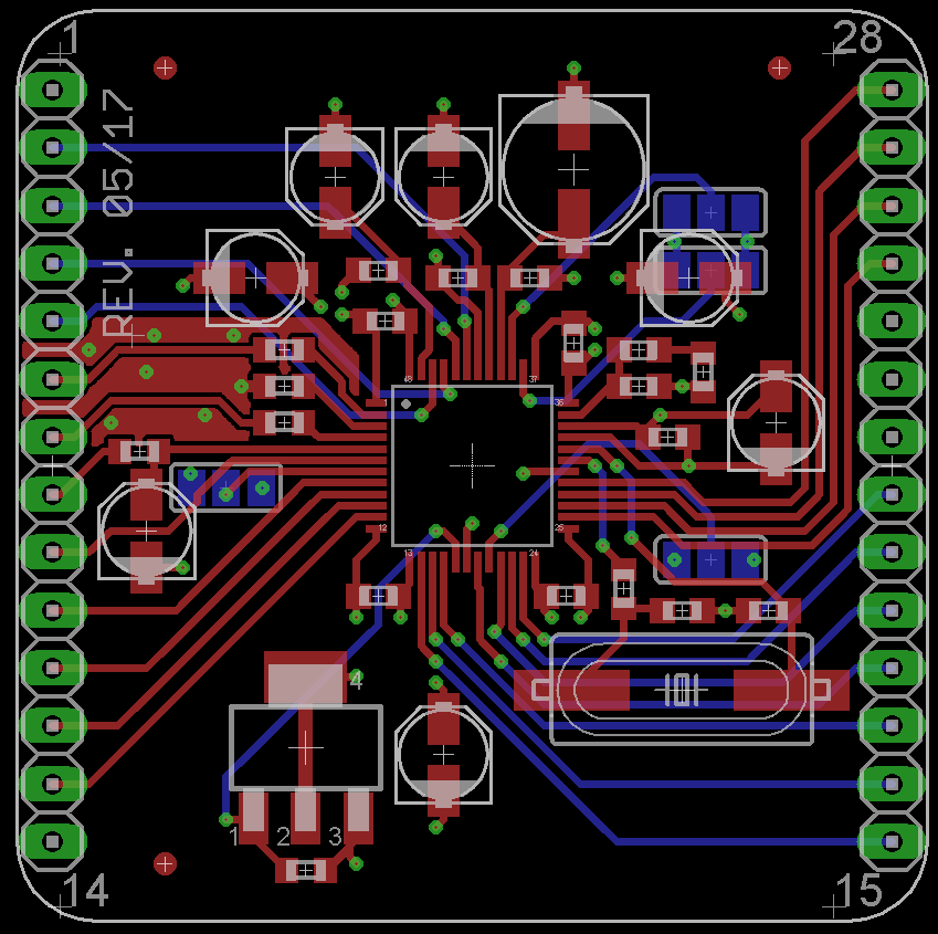
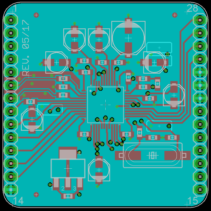
So I think I made some sensible changes to my layout. I removed the top and bottom GND-fills, except in the area of the ADC-inputs, to reduce crosstalk.
I routed all the VDD and GND pins very carefully to the corresponding caps. I also had a look at the documents about the placement of parts and so I shifted the crystal as much as possible towards the chip. Maybe this will also do a good job.
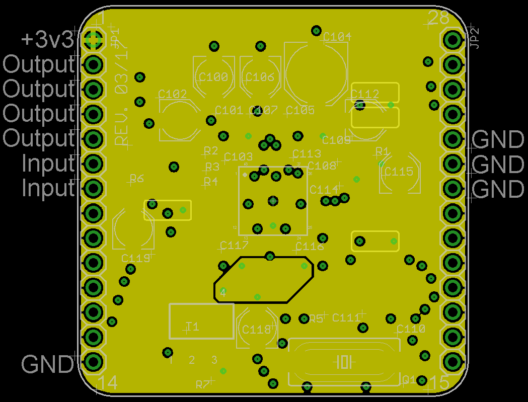
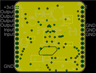
To make clear, how things are arranged now, here I made some pictures of the situation:
Top and Bottom - Top and inner GND - Top and inner supply
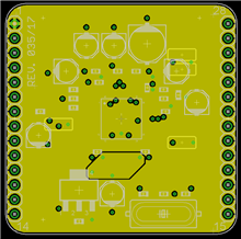
And here I highlighted all pads, connected to GND:
So, I think none of the pins that could draw current and pump noise into the GND-plane is connected directly to GND anymore.
Can you throw one more glance at it and give a quick advice, if there is still something, I should do before I start a test?
Thanks a lot,
Hanno
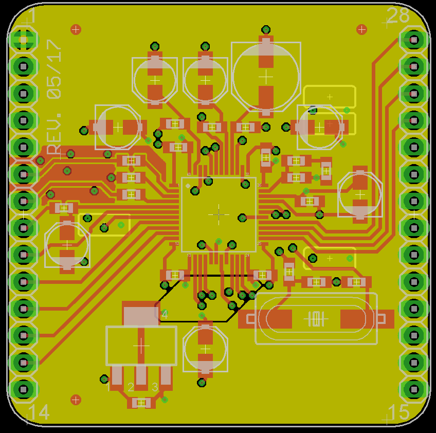
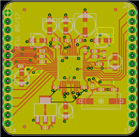
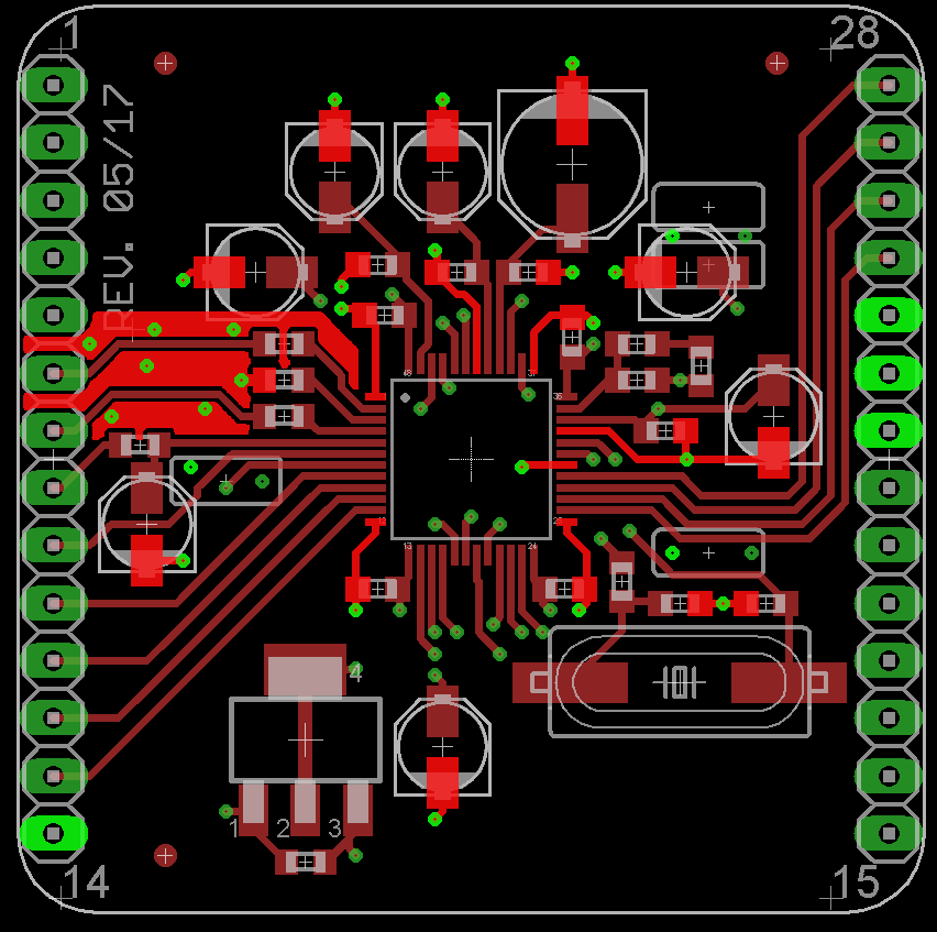
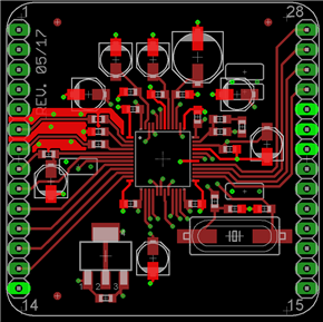
While I agree with Dave that the decoupling caps for the ADAU1701 should have their ground connections routed differently, I think you might be chasing a goal with this DSP that you will never be able to achieve. As nice as the ADAU1701 is with its integrated ADCs and DACs, those sections are far from state of the art and likely responsible for the majority of the system noise floor. You can test this by turning off the ADC section of the DSP and checking the reduction in noise floor. I ran into this same issue after using the ADAU1701 in a number of less critical projects and when a new project came up that had requirements for a far lower noise floor, I moved to an ADAU1446 with high quality external ADCs and DACs.
Hello Hanno,
It seems like noise is often an issue when building powered speakers, for two reasons:
User-provided input is rarely at optimum level, throwing away some available dynamic range.
Often the speakers are set up in quiet surroundings where the ADC noise appears objectionable -- even though when in actual use, no one ever notices it amid the ambient sound.
I'm afraid that audiolab1's comment is correct -- there are better ADCs than what's in the ADAU1701. An external codec would provide a much lower noise floor. To run at 96K, you'll need to find a codec that features standalone operation at that rate -- or else include a microcontroller in your design to configure the codec.
I'm curious if the circuit that U.E. presented, https://ez.analog.com/message/297956 would prove quieter than the standard -1701 ADC input circuit, although I haven't tried it myself.
Finally, it may help enough to directly address the issues I outlined above:
Provide an input level control with some gain before the ADAU1701, along with a "clip" LED to assist in finding its proper setting -- thus using as much dynamic range as possible.
You could "cheat' by including a noise gate in your Sigma Studio flow. It would attenuate the audio by an additional 10 dB (for example) at very low input levels, making the speaker appear quieter than it really is while it's being set up at a gig.
There's been some fascinating if extreme solutions on these boards, such as this one:
https://ez.analog.com/message/66292?commentID=66292#comment-66292
Best regards,
Bob
Hello Hanno,
I would like to put an additional idea into the discussion.
At first, if you leave the adc inputs open, you will get only the noise floor of your system. Now you should clarify if the noise present in both channels is correlated. This may be done by a small program which subtracts both internal adc signals and put the level to a level meter. The same has to be done by adding the adc channels. Provide highpass filtering (2nd order 100Hz) to remove DC offset in both cases and appropriate gain of at least 40dB.
If addition level is much greater than subtraction level your problem is related to GND noise. If the levels are comparable your problem may come from a jittery clock.
You may also identify whether the noise floor has some peaking at discrete frequencies to get some new ideas for troubleshooting.
For myself I have paid special attention on the ADC REF resistor. Connect it on the shortest way between pin 1 and 3, it has to be 18k.
Another point would be to try 48kHz sampling rate and checking the difference between performance at 96kHz. If there is a big deviation clock is likely the problem.
Good luck, hope it helps a little bit..
Best regards Ulli
Please log in to reply.