Question about ADAU1452 PCB layout
Hello all,
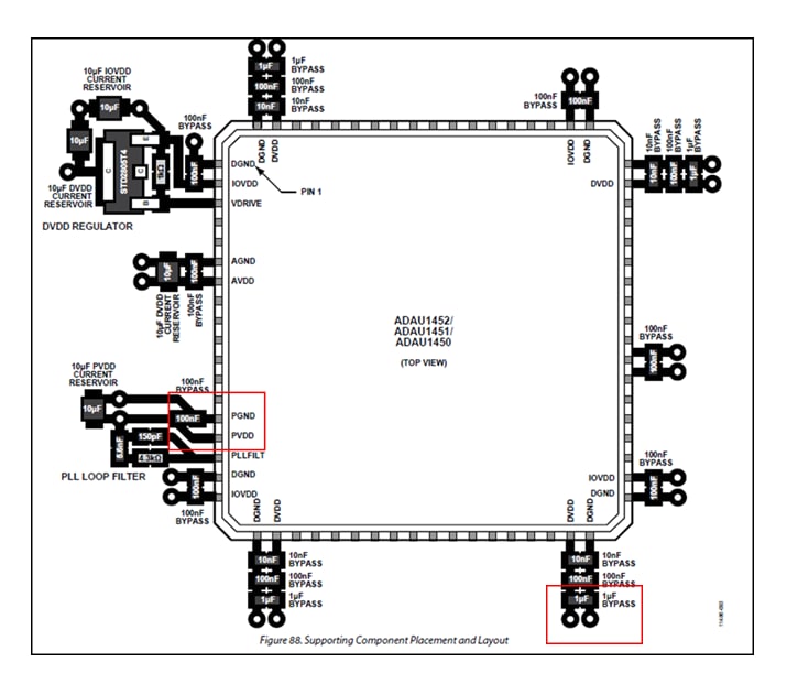
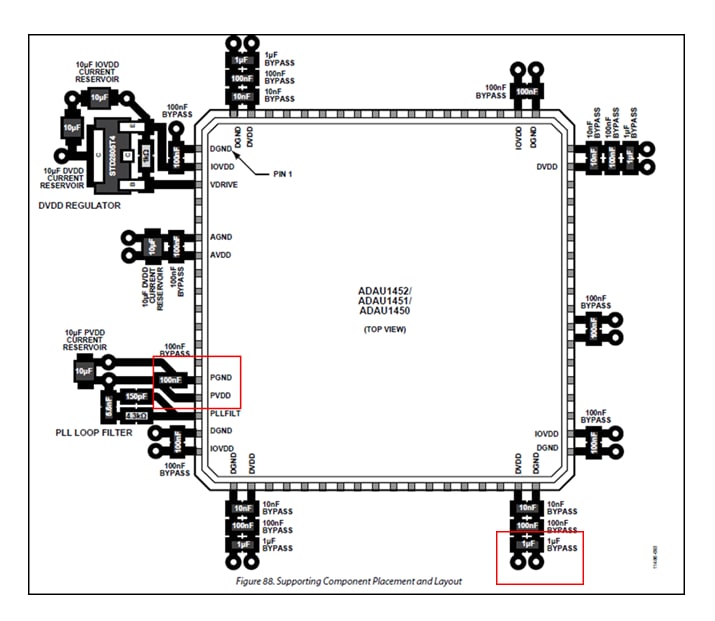
I have 2 questions on the figure below.
Question1
On the red box on the left side,
the 100nF cap is placed near to the GND not the PVDD as recommended on "Figure 81. Recommended Power Supply Bypass Capacitor Layout".
Is it okay?
Question2
On the red box on the bottom right, 1uF cap is newly appeared.
what is this for??? Is this just a typo and you wanted to mean 10uF cap?
On page 178, there is even a description as below
"The 1 μF bypass capacitor is required to provide a local current supply for sudden spikes in current that occur at the beginning of each audio frame when the DSP core switches from idle mode to operating mode."
However, on page 176, you mentioned as below
"To provide a current reservoir in case of sudden current spikes, use a 10 μF capacitor for each named supply (DVDD, AVDD, PVDD, and IOVDD) as shown in Figure 83."
To prevent the current spikes, which cap should we need, 10uF or 1uF?
Best Regards,
Yuta M
Audio Signal Processors
adau1452
SigmaDSP Audio Processors
Hello Yuta,
Question 1:
It does not make that much of a difference. You can rotate the cap 90 degrees and have the cap be the same distance from the pins if you like but the important thing is that there are no vias between the cap and the pins.
Question 2:
I did not write this datasheet so my opinion is that it is a matter of design preference. If the power supply regulator is not close by then these 1uf caps is probably a good idea. If you need to save costs then having a 10uf cap on the board reasonably close by will probably be good enough. So this is your choice. These are a suggestion.
The important thing shown in this example is where to place the 10nf and 100nf caps and where to place the vias to the power and ground plane. This is very important.
Dave T
Please log in to reply.