ADAU1452 Power up sequence
Hello all,
I have 2 questions on the power up sequence of ADAU1452.
Question 1
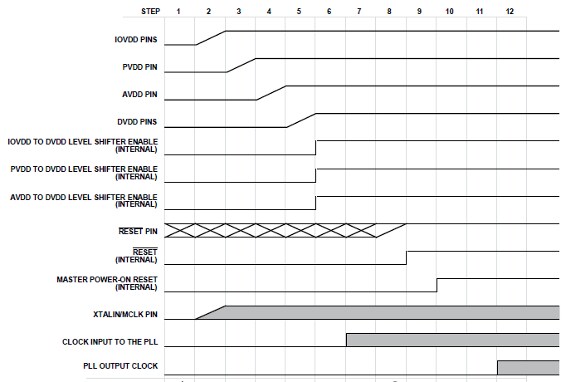
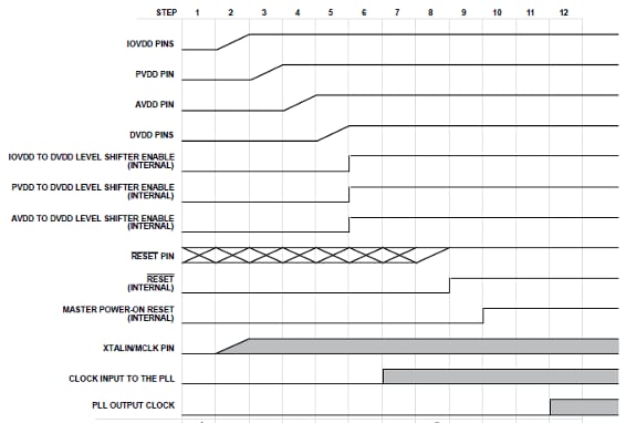
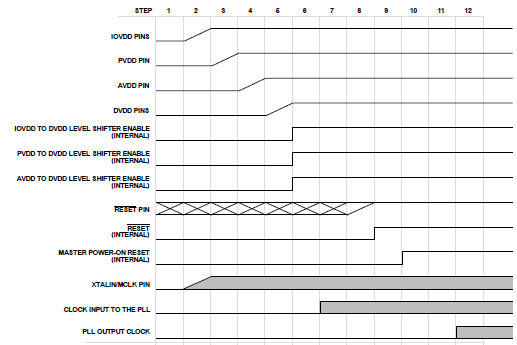
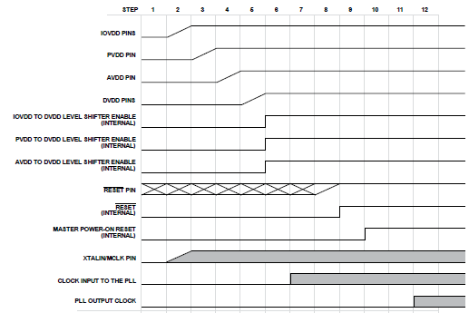
On the datasheet p.25, the description of the step 8 says as below.
"IF THE RESET PIN IS NOT ALREADY HIGH, PULL IT HIGH AT ANY TIME.(AT THE BEGINNING OF A POWER SEQUENCE, THE STATE OF THE RESET PIN IS DON’T CARE.)"
However, Step 1 says "STARTING CONDITIONS. ALL SIGNALS ARE LOW."
the state of the reset pin is still "Don't care" even if the step 1 says as above?
Question 2
The step 10 states as below.
"WHEN THE INTERNAL RESET GOES HIGH, THE DSP CORE RUNS INITIALIZATION CODE, WHICH REQUIRES EIGHT CYCLES OF THE XTALIN/MCLK SIGNAL.AT 12.2888MHz,THE PROCESS REQUIRES 650ns."
From which event should I wait for the 8 cycle? By which trigger can I recognize the processing time of 650ns starts and ends?
Best Regards,
Yuta M
Audio Signal Processors
adau1452
processors and dsp
SigmaDSP Audio Processors
Processors and Microcontrollers
Hello Yuta,
Question 1: Most of those signals shown are internal so therefore they will be low upon the initial condition before power is applied. It does show that the reset pin does not matter if it is high or low. The datasheet did specify that about the reset pin but he did not write the detail again in that one sentence which was intended to say that all the power inputs need to be low and the internal signals will be low. So you have found the exception. The reset pin does not matter until the PLL has a clock input and enough time has passed for the initialization.
Question 2: I do not think there is any way to know exactly when this trigger event has happened. Some of these events are not something we have control over like how fast the power supplies come up. So there is a certain amount of time that we cannot exactly account for. When crystals start up they often slowly come up to a good signal level. So which cycle does it actually start clocking the part is also variable. This is all detailed to give you an approximation of the time it takes for the part to start up and begin loading a program or to be available to load in a program from a system controller. These times and variability I am talking about is very small amounts of time and usually is not a problem. Your question about having a flag to know when the DSP is running is a great question and that is the best way to implement the wait for the system to be up and running.
Dave T
Hello Dave,
Thank you for your answer.
The question 2 is now clear.
I still want to ask you a further question on the question 1.
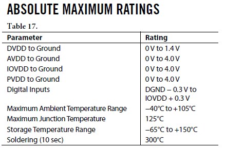
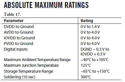
The datasheet p.17 has Table 17 as below.
According to this table, the absolute maximum of the "Digital Inputs" is defined in the range "DGND-0.3V to IOVDD+0.3V".
During STEP 1 and 2 on the figure above, IOVDD is 0V.
This means the absolute maximum of the digital input would be 0.3V(0V of IOVDD + 0.3V).
Pulling reset pin High during the step 1 and 2 viorates the absolute maximum, doesn't it?
Best Regards,
Yuta M
Hello Yuta,
Yes it does mean that having a signal on a pin while IOVDD is off (0V) will violate the absolute max on the pins. I have seen clocks keep a part alive when power was removed by forward biasing the ESD diodes. This was on our really low power parts not this part. But still, you are good to notice that you cannot apply signals on a part if you have the power gated. I know that this customer will have the DSP in a larger system where power will be gated to this board until it is needed. So some signals will be live when the DSP is powered down.
The solution is to identify external clocks and signals that will be on when the DSP is off. Then use a level shifter to isolate the two power domains. So when the DSP IOVDD is gated off, the level shifter will shut down the signal to the DSP. It is extra parts and effort but it would be required in this sort of application.
Dave T
Please log in to reply.