Recommended land pattern for ADAU145x?
Surprised it isn't on the datasheet. Is there a simple drawing of a recommended land pattern available?
Hello,
You'll find package, layout and soldering info in application note AN-772.
Package Resources | Design Center | Analog Devices
Best regards,
Bob
Thanks. That's a pretty detailed document, and I see how to derive the pattern, but why not just publish a simple drawing? I'd think that would be less susceptible to error.
I think the AN-772 is a good starting point, but the land pattern is also related to solder process.
While prototyping (reflow), i like to expand the pads a bit, cause it is easier for rework or for example to probe a signal.
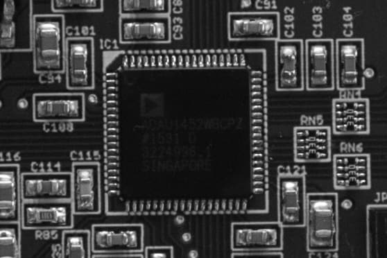
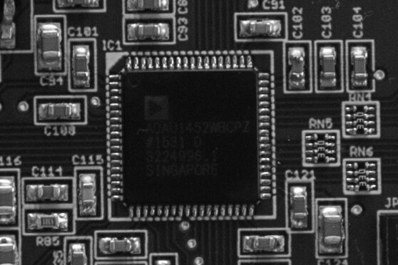
Hello Joe,
Yes, a drawing specific to the ADAU145X would be handier than the generic one in the ap note. There's also a CAD file atSymbols & Footprints | Design Center | Analog Devices -- I don't know if it is useful.
Thanks. Having the drawing of the part on the datasheet is certainly worthwhile, but omitting the land pattern is puzzling. Why would ADI do that? Including this info is pretty common practice, and is especially important for such a dense part with critical thermal properties.
I was hopeful that the CAD you posted would work for verification, as it seems promising, but it appears erroneous: the pads and soldermask are much wider than recommended by AN-772, leading to no soldermask between pins, which invites solder bridges.
Also puzzling is why the gerbers for the EVB aren't available. The pattern is also different than suggested by AN-772, but as least we know they're successful. Why aren't these published? Can someone from ADI just post them?
Heidi -- I like the picture and your idea of longer pads for probing. Not enough folks think about this. On my job I end up troubleshooting a menagerie of boards, each year with tinier features than the previous. It's making me feel as old as my avatar!
Joe -- Sometimes ADI has been willing to provide eval board Gerbers, and sometimes not -- compare these links:
EVAL-ADAU1701MINIZ Could Analog Devices please supply the Gerber files for this board
1452 Evaluation Board Gerber files?
Thanks! Great photo, Heidi.
I guess I'll await a reply for ADI regarding the Gerbers. Otherwise I'll wing it.
One other question, if I may: How elaborate do you get with the stencil design and vias detailed on AN-722? Segmented stencil with plugged vias? Or something simpler? It's hard to tell what's done on the EVB, but it looks like they used a thermal relief.
(The gerbers sure would be helpful!)
The recommend land pattern for thermal pad is described in AN-772.
Just read it, this is not rocket science.
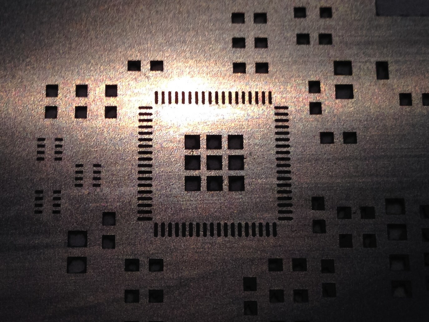
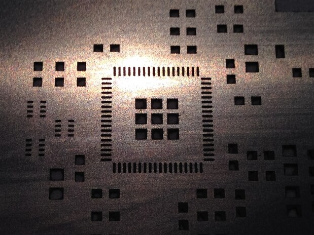
AN-772 does provide useful information in designing a custom land pattern and stencil, but it is much simpler, and less prone to error, if this information were provided directly, as seems to be the case with many other vendors. Putting a pattern at the end of the datasheet is standard practice, and I'm uncertain why it's not done here.
Please log in to reply.