EVAL ADAU1772 communicating with FPGA
Hi I just purchased an evaluation board from the ADAU1772 and need a bit of help.
I want to the use the ADAU1772 to communicate with a FPGA to transmitt the data from the ADC to the FPGA and transmit data from the FPGA to the DAC. I have programmed an I2S interface in VHDL which runs without problem. The problem comes when connecting the FPGA to the ADAU1772.
I have been using the ADAU as a Master to transmit the data to the FPGA. My question is what to do with the MCLK signal?. My guess was that I should use the FPGA to provide the CLOCK signal to the board using that MCLK line. In the documentation is written that to use an external clock, the R3 should be removed from the board. I have done that, and I am generating a CLOCK signal with the FPGA of 10MHZ. How should I configure the ADAU1772 with SIgma Studio to use this external MCLK?
Does anyone have an aidea how to do this?
adau1772
Integrated/Special Purpose A/D Converters
Audio CODECs
Hello Jose,
This part has some interesting differences from most other codecs/DSPs. The intended signal path that was most critical for this design was the ADCs to the DSP to the DACs. This needed to be fast (low latency) so they are all clocked at a high rate. The serial ports are there for use if needed and cannot be setup to slow down the rest of the system. So the serial data in and out of this part go through sample rate converters. This makes interfacing quite easy.
You can run the 1772 as a master or slave but in your case I think you should run it as a slave. This way the 1772 will run using its own clocks oblivious to the rest of the clocking on your board. Then you only need to send it BCLK and LRCLK (and Data of course) and it will figure out the sample rate difference and convert it to the DAC sample rate and convert the ADC sample rate to the incoming clocks. It is a lovely thing, it just works.
So reconnect the MCLK on the eval board using the 12.288 MHz crystal and let it run from that clock.
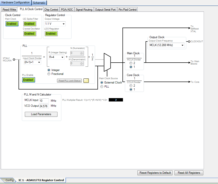
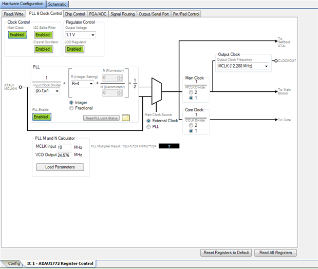
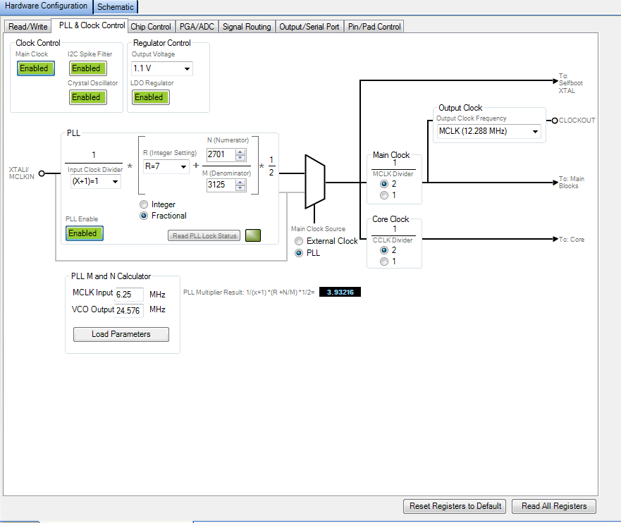
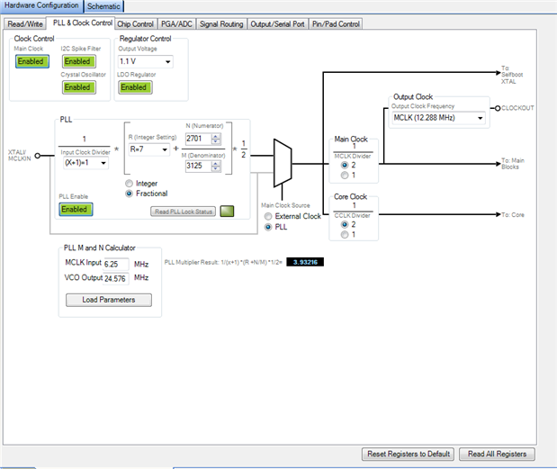
Now, in your final design you can certainly use the 10 MHz clock from the FPGA. All you will have to change at that point is to use the PLL to increase the 10MHz up to 24.576MHz. This is all explained in the PLL section of the datasheet. You will have to set it up in factional mode. I see by the screenshot that you started that process. You entered 10MHz into the handy PLL calculator. When you click "load parameters" it will load in R=4, N=572 and M=625. These will setup the PLL to multiply the 10MHz by 2.4576 to get 24.576MHz. Then you will need to enable the PLL, then set the main clock source to "PLL" and then set the main and core clock dividers to 2.
Dave T
Many thanks Dave for the explanation,
I have reconnected the resitor back to the board (not without problems, but that's just my lack of ability when soldering).
Working as a salve I have to generate the BCLK and LRCLK with the FPGA, right?
Thanks and sorry to bother with probably stupid questions
Many thanks!
Nice device this ADAU1772
Cheers
Hello Jose,
Yes, you have to generate the BCLK and LRCLK with the FPGA.
Dave T
Hi Dave.
Sorry to bother you again.
I am trying to do what I explained before, use the data from the ADC, pass it through the FPGA and then feed it to the DAC. I am using the I2S format, and to do so I have an interface programmed in VHDL which seems to work fine.
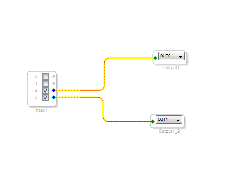
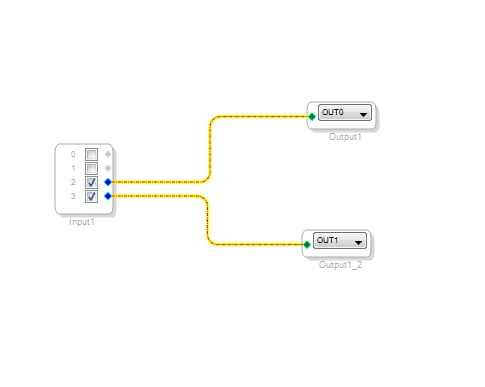
Right now I am feeding the stereo input AIN2/3 with an audio signal (comes from my cellphone), and in the stereo ouput I am using a headset. Below is the schematic
As you told me I am using the ADAU1772 in slave mode. I am using external BCLK and LRCLK signals generated from the FPGA. I am using the clock signal from the FPGA board divided by 16 as BCLK signal (100MHZ/16=6.25 MHz). I could use a faster BCLK, but I don't know if that has an influence.
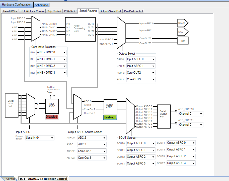
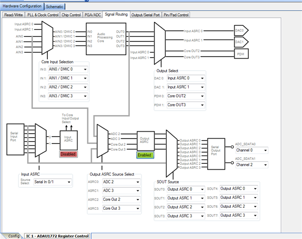
In the signal routing tab i have done the following: the output ASRC Source Select, I have taken ADC2 and ADC3 as ASRC0 and ASRC1 and I have enabled the output ASRC. My guess is tha both signals from ADC2 and ADC3 will be then in the port number 10 from the serial audio interface header J4 labelled as ADC_SDATA0, is that right?.
This signal will be read by the FPGA board. The FPGA board generates also a I2S signal which I assume that has to be connected to the port number 8 from the J4 labelled as DAC_Sdata.
Besides I have also linked in the ouput select to DAC0 the signal from input ASRC0 and to DAC1 the signal from ASRC1. With that I assume that the signal received in the port 8 will be transferred to the DACs, is that correct?
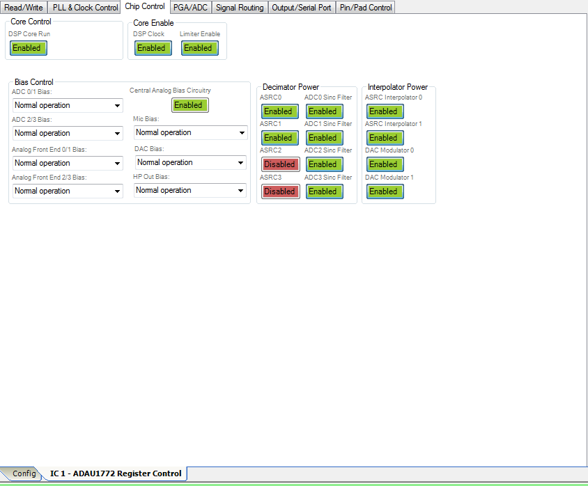
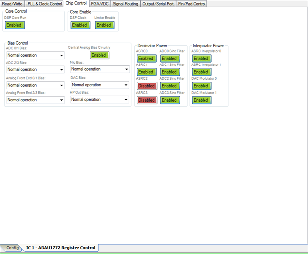
In the chip control Tab I have used this configuration. I dont know if that is correct. I have enabled decimator from ASRC0 and ASRC1, as well as the interpolators and DAC modulators.
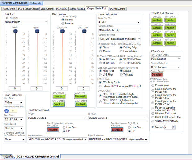
Finally in the output serial port tab, I have set the mode to I2S and the ADAu as a slave. Should I do something else?
I don't know if I am making a mistake somewhere but it is not working properly with the PLL configuration. If I change to external clock, I hear the sounds, but with the PLL activated, i get no audio. I have been checking also with a scope, and with the external clock I see "active signals", they are changing with the music, and with the PLL I see what it looks as proper I2S signals, but they don't change.
Many thanks for your help and sorry for the long text

Many thanks for your response.
I am refering with port 8 and 10 to the serial audio connector of the jumper 4. which is the serial audio connector. You are right, I want to bypass the core, and do some calculations within the FPGA, but right now I am not doing any.
You are right, I didn't have the input ASRC activated, but it still doesn't work with the PLL. The funny thing is that it does work with the external clock as clock source, even without the input ASRC enabled, which in my opinion it doesn't make too much sense. Actually since in this case I am not modifying the audio signal with the FPGA yet, if I change the output select of the DAC0 and DAC1 to COREOUT0 and COREOUT1 (which will route the signal through the core, but th core is also not doing anything) I hear the same sound as when I am setting the output to INPUTASRC0 and 1.
Thanks again
Hello Jose,
I don't understand what you mean when you say port 8 or port 10?
You do not have the input ASRC enabled. So you will not get any data to get up to the DAC.
Otherwise, I do not see any other issues with register settings. You will not be going through the core with these settings but I think that is what you are intending.
Dave T
Please log in to reply.