Clarification on ADAU1701 pin 10 & 11
Hello,
With reference to the ADAU1701 datasheet Rev. B, page 11 states for:
Pin 10: Serial Input Port Data 1 (SDATA_IN0)
Pin 11: Serial Input Port Data 0 (SDATA_IN1)
This is a little confusing.
Kindly clarify which pin is assigned to SDATA_IN0 and SDATA_IN1.
Thanks in advance!
Ravindra.
Audio Signal Processors
SigmaDSP Audio Processors
adau1701
Hello,
Pin 11 is SDATA0 / TDM. I know because I had to move this connection on a prototype.
Best regards,
Bob
Thank-you Bob for the quick reply.
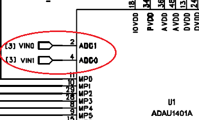
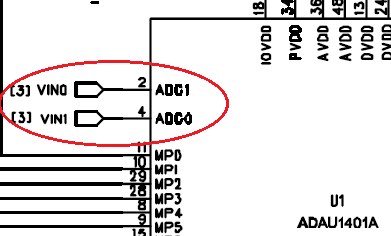
I am also confused about ADC0 (Pin2) and ADC1 (Pin4).
The EVAL-ADAU1701MINIZ.pdf has the pins swiped.
Thanks in advance and regards,
Ravindra.
Hello Ravindra,
Fortunately if you committed a design to copper and then found flopped interconnects such as this, a trivial software fix (flopping the two ADCs in your SigmaStudio flow) would resolve it.
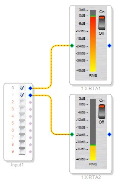
This brings us to which ADC hardware pin actually relates to ADC0 in the SigmaStudio schematic. A test reveals the following:
The eval board is wired according to its schematic (IC pin 2 connects to R15 & C35, etc.).
Placing an audio signal from the "left" channel of my laptop to the board puts audio on C35, hence pin 2.
That signal shows up at ADC0 in the signal flow.
Thus, the data sheet (which describes pin 2 as ADC0) is correct. ADC1 is indeed pin 4.
Best regards,
Bob

Thanks again Bob for your quick reply.
The design is still in schematic phase and I was just looking into the details to ensure a first time right proto and you are certainly helping me get there!
Regards,
Ravindra.
Hello Ravindra,
Thank you for your appreciation! Perhaps there's an explanation for why the legends ADC0 and ADC1 are flopped in the ADAU1701 as it appears in the eval board schematic. Looking at UG-072, describing the eval board for the pin compatible ADAU1401, the identical mistake appears in its schematic.
Likely the mistake occurred in the CAD symbol for these parts, and then propagated to any application schematic. Though it has no lasting effect on the operation of your prototype, I appreciate your desire to get everything right.
Best regards,
Bob
Please log in to reply.