My DSP/DAC Project
Hey guys...
My first post on here and possibly quite in over my head here, but want to do something crazy.
I want to build a DSP / DAC combo based on TWO ADAU1445 and 2 ADAU1966.
The processors will be booted via I2C from a SAM3X8E. I'm trying to run them double precision and Master / Slave configuration.
The reason why I picked the Atmel SAM3X8E unit is quite simple...
It has default USB, Ethernet and SD Support, easily interfaced with an LDC with multiple libraries available and last but not least is easily programmable thanks to being used as the main processor in the Arduino Due.
The hardware part is going to be fairly easy compared to the software/firmware in my mind. So far I have made a schematic for the 1445 using the I2C diagram from the datasheet ( page 90) and starting with that.
Also because its most likely going to be an "evolving" project I would like to have all the signal pins available, and by that i mean the all the inputs being brought to the edge of the board as well as unused output pins that aren't tied to the DAC will be brought back to the edge. the DAC output will be brought to the edge of the board to individual 3pin headers. This way I can choose my output section accordingly to amp its being fed into
I worked on it a bit yesterday and was able to come up with this:
Audio Signal Processors
Audio Products
Audio D/A Converters
adau1445
SigmaDSP Audio Processors
adau1966
Show More
I'm starting today on the DAC section today and most likely apply the same concept of decoupling and filtering as for the 1445.
Any input would be greatly appreciated!
Hello Adrculda,
I see what you are trying to do, leave yourself a lot of flexibility. I will mention a few things you may want to do to give yourself some more flexibility.
First of all, you will need to connect the ADDR0 and ADDR1/COUT pins to either GND or IOVDD to set the I2C address. Since you plan on having multiple parts on the I2C buss then it would be wise to either use DIP switches or 0-ohm jumpers to set the address of each board.
I noticed that you are running the CLKOUT pin out of the board yet you have the CLKMODE pins set to disable the CLKOUT. So again, you will probably want to use some 0-ohm jumpers to give yourself the flexibility to change the CLKOUT rate if you need to.
I would do the same with the PLL0, PLL1 and PLL2 pins. The setting you have is fine but in case you need to change it make it simple to do.
With the exception of the CLKOUT pin, you have no master clock distribution. Having the CLKOUT is probably enough for you and the ADAU1966 does have the ability of running with only the LRCLK and DATA and will use its own PLL to synthesize the clocks it needs. However, it is good to have the option of running using MCLK, BCLK and LRCLK.
You will need to allow for the fixing of signal integrity issues. The most simple way is to have a series resistor on all the clock and data lines. The exact value depends on the PCB stackup, the length of traces, the drive strength of the driving part, the number of vias used etc.etc. Generally it is anywhere from 10-ohms to 50 ohms. This will be important if you want clean glitch-free audio. You will need to have power and ground planes on your PCB and you will need to layout the bypass caps properly. I think there are other posts on this forum that goes into more detail. Some engineers know about all this and some do not so let me know if I need to point you to more information. Do be aware that you will not be able to run the clock and data lines very far off of this board. It will depend on the cable used and if you are running ground on every other pin and the connectors used etc. The ADAU1445 does have an adjustable drive strength but it is not intended to be a buffer. So you may want to buffer these lines if you plan on driving anything more than a few inches of cable.
One more thing. I see you are using 3.3V AVDD. Are you planning on using 3.3V AVDD for the ADAU1966? If so then you will need to use the ADAU1966A instead because that part is rated for 3.3V operation. Are you planning on running differential out of the DACs or single-ended? The ADAU1966 is differential only where the ADAU1966A is both.
Thanks,
Dave T
Thanks for the Input Dave!
Added dip switches and changed a few things around...
Now possible for both I2C and SPI communication.
I'm basically splitting whole schematic into sections so it doesn't clutter up and cuts down re-drawing the whole schematic by only drawing out half and then mirroring the second device from the first sheet.
This way each sheet is represented as a module in the main wiring diagram as shown above.
I2S data and clocks lines will use UFL connectors and cables on all inputs and outputs as the DIYAudio community likes these for its low profile, price point and performance also they are going to routed to another board which will re-encoded to SPDIF ( Coax, Toslink and AES/EBU )
The power supply will be modular and fully regulated ( followed by a CLCRC section ) and separate 3.3V and 5V supplies are going to be available for each "processor". Only on board regulators are going to be for 1.8V and 2.5V and those are to AD's specs.
I have some comments in addition to what Dave T recommended.
Here are a few notes and thoughts I have after reviewing your schematic:
ADDR0 (pin 20) must be either grounded or pulled to IOVDD, depending on the I2C slave address you want. See page 26, Table 13 and Table 14 in the datasheet for more details.
ADDR1/CDATA (pin 20) must be either grounded or pulled to IOVDD, depending on the I2C slave address you want. See page 26, Table 13 and Table 14 in the datasheet for more details.
I would recommend setting DSP1's I2C address to 0x70 (ADDR1 = GND, ADDR0 = GND), and setting DSP2's address to 0x72 (ADDR1 = GND, ADDR0 = IOVDD). That will allow you to access them separately using the microcontroller's master I2C port.
If you want to send a 12.288 MHz master clock signal from the ADAU1445's CLKOUT pin to the ADAU1966, which I would recommend, then CLKMODE0 (pin 30) should be tied to GND and CLKMODE1 (pin 29) should be tied to IOVDD. See page 23, Table 10 in the datasheet for more details.
It might be a good idea to put a weak pull-down to GND (10 kOhm or so) on the RESET line (pin 54), so that the device is in reset even if the microcontroller releases the reset line.
Dave T, I think the AVDD in this schematic is used for the auxiliary ADCs on the ADAU1445, which appear to not be in use. So, this isn't the same AVDD that will be used with the ADAU1966s. As such, I think it would make sense to give those nets separate names (1445_AVDD and 1966_AVDD, for example).
Here's a question for Adrculda: will all of DSP1's outputs go to DAC1, and will all of DSP2's outputs go to DAC2? If so, that simplifies clock routing. If not (in other words, if some digital output data is shared between the two DSPs), then there will be a little bit of decision-making involved in figuring out clock distribution, but we can help you with that.
Thanks for the input Yagami.
But there is a bit more treachery a foot here..
Here's a quick road map:
DSP1:
BLCK0/RLCLK0 -> BLCK2/RLCLK2 : I2S Input From Digital Input Board ( DIX9211 )
BLCK3/RLCLK3 -> BLCK5/RLCLK5 : I2S Input From DSP2
BLCK6/RLCLK6 -> BLCK8/RLCLK8 : I2S Output To DSP2
BLCK9/RLCLK9 -> BLCK11/RLCLK11 : I2S to Digital Output Board ( DIT4192 )
DSP2:
BLCK0/RLCLK0 -> BLCK2/RLCLK2 : I2S Input From Digital Input Board ( DIX9211 )
BLCK3/RLCLK3 -> BLCK5/RLCLK5 : I2S Input From DSP1
BLCK6/RLCLK6 -> BLCK8/RLCLK8 : I2S Output To DSP1
BLCK9/RLCLK9 -> BLCK11/RLCLK11 : I2S to Digital Output Board ( DIT4192 )
DSP1 -> DAC1: SDATA0 - SDATA4
DSP2 -> DAC1: SDATA0 - SDATA4
DSP1 -> DAC2: SDATA5 - SDATA8
DSP2 -> DAC2: SDATA5 - SDATA8
Clocks to the DAC's will be supplied from a single LMK00334 Fan out buffer which in turn will be fed from a Crystek CCHD957 ( 12.288MHz - Not listed but a custom ). Each DAC will feed the clock to its subsequent DAC.
Again, I'm not worried about the hardware as much I'm worried about the software
My main concern is the I2C boot of multiple processors from a single MCU.
Along with separate Register Information and Settings for each individual one is what I'm confused about.
Slave Addressing will be as follows:
DAC1 - 0x04 ( ADDR1 - 0, ADDR0 - 0)
DAC2 - 0x24 ( ADDR1 - 0, ADDR0 - 1)
DSP1 - 0x70 ( ADDR1 - 0, ADDR0 - 0, Read/Write 0)
DSP2 - 0x72 ( ADDR1 - 0, ADDR0 - 0, Read/Write 1)
[quote=Me]
Clocks to the DAC's will be supplied from a single LMK00334 Fan out buffer which in turn will be fed from a Crystek CCHD957 ( 12.288MHz - Not listed but a custom ). Each DAC will feed the clock to its subsequent DAC.
I decided to go against it and use the kiss rule.
DSP1 and DSP2 will have their own clock and feed MCLK the subsequent DSP's.
Also instead of crossing DSP signals I pulled the unused outputs to the side of the board and those can be routed back and forth if needed VIA an external jumper board.
DSP's have 50Ohm resistor networks on input as suggested in earlier post.
OK, well now this is getting more interesting!
Let me try to break down the problem here. I find it easier to collect my thoughts by writing them down...
DSP1 has two input clock domains - DIX9211 and DSP2.
DSP1 has two output clock domains - DSP2 and DIT4192.
Let's start with DSP1.
It would be easiest if DSP1's outputs could be masters. This would mean that DSP2 and DIT4192 would be slaves to DSP1. Therefore, on the input side of DSP1, only one set of ASRCs is needed to handle the asynchronous input from DIX9211.
SDATA_IN0, SDATA_IN1, and SDATA_IN2, will be slaves to the clocks coming in on BCLK0/LRCLK0, BCLKIN1/LRCLK1, and BCLK2/LRCLK2. The data from SDATA_IN0 goes to ASRC0. The data from SDATA_IN1 goes to ASRC1. The data from SDATA_IN2 goes to ASRC2.
SDATA_IN3 (BCLK3/LRCLK3), SDATA_IN4 (BCLK4/LRCLK4), and SDATA_IN5 (BCLK5/LRCLK5) will be set up as masters. Their clock pins will be routed to the corresponding pins (BCLK6/LRCLK6, BCLK7/LRCLK7, BCLK8/LRCLK8) on DSP2.
SDATA_OUT6 (BCLK6/LRCLK6), SDATA_OUT7 (BCLK7/LRCLK7), and SDATA_OUT8 (BCLK8/LRCLK8) will be set up as masters. Their clock pins will be routed to the corresponding pins on DSP2 (BCLK3/LRCLK3, BCLK4/LRCLK4, BCLK5/LRCLK5).
SDATA_OUT0 (BCLK9/LRCLK9), SDATA_OUT1 (BCLK10/LRCLK10), and SDATA_OUT2 (BCLK11/LRCLK11) will be set up as masters. Their clocks will be routed to the DIT4192.
OK, now on to DSP2.
SDATA_IN0, SDATA_IN1, and SDATA_IN2, will be slaves to the clocks coming in on BCLK0/LRCLK0, BCLKIN1/LRCLK1, and BCLK2/LRCLK2. The data from SDATA_IN0 goes to ASRC0. The data from SDATA_IN1 goes to ASRC1. The data from SDATA_IN2 goes to ASRC2.
SDATA_IN3 (BCLK3/LRCLK3), SDATA_IN4 (BCLK4/LRCLK4), and SDATA_IN5 (BCLK5/LRCLK5) will be set up as slaves to DSP1.
SDATA_OUT6 (BCLK6/LRCLK6), SDATA_OUT7 (BCLK7/LRCLK7), and SDATA_OUT8 (BCLK8/LRCLK8) will be set up as slaves to DSP1.
SDATA_OUT0 (BCLK9/LRCLK9), SDATA_OUT1 (BCLK10/LRCLK10), and SDATA_OUT2 (BCLK11/LRCLK11) will be set up as slaves to DSP1. You'll need to route the appropriate clock signals to those pins. These clocks are copies of the clocks being routed to the DIT4192.
Now, it's important that DSP1 is set to have its DSP Start Pulse internal (since it is the master) and to have DSP2 set its DSP Start Pulse to come from a serial port that is a slave to DSP1. This will put the two DSP cores in sync, I think.
So, with those recommendations, I think you're all set.
Whoops, I just saw your updated post. I agree, keeping it simple is best. Having each DSP be independent and not crossing data lines keeps a lot of complexity out of the design.
As far as addressing multiple devices in the system is concerned, it's quite simple. Every I2C message starts with a chip address byte. All you need to do is change the chip address byte every time you're accessing a different slave device on the I2C bus. SigmaStudio can help you generate your microcontroller code, or at least a big part of it (see here for more details: How do I create the microcontroller code to interface to my SigmaDSP?). You'll notice that in the exported files from SigmaStudio, there is a definition for the I2C address. You just need to change the address to match what's in your actual hardware.
You can also take care of this in SigmaStudio by setting the proper addresses on the USBi. Check out the "Configuring the USBi to communicate with multiple ICs" section on page 4 of the USBi application note, here: http://www.analog.com/static/imported-files/application_notes/AN-1006.pdf
Thanks for the input Yagami.
This is what I had in mind...
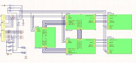
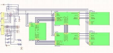
This way the DSP1 can generate clocks for all subsequent chips and and only 1 crystal is required this way.
DSP1 will handle ASRC and signal routing to the other 2 DSP's
As you can see all DSP's have 4 data lines tied to each other for easy signal routing to each DAC.
Each data line is configured TDM4 ( 4x TDM4 nets me 16 channels which is what I'm for each DAC ). Input to DAC1 is setup with 4 input data lines with their corresponding MCKL and LRCLK's and each input is set as Flexible TDM Mode.
The extra inputs are just there just in case i would like to add either a CobraNet processor, USB audio or just another DIX9211 to handle those extra inputs and add the on as a second channel.
With I2C in control I can easily set up a input switch and use I2C to switch between the 2 chips.
Just an example:
Chip1 - Input 1 - Coax SPDIF
Chip1 - Input 2 - Coax SPDIF
Chip1 - Input 3 - TOSLINK
Chip1 - Input 4 - TOSLINK
Chip1 - Input 5 - USB Audio
Chip2 - Input 6 - AES/EBU
Chip2 - Input 7 - AES/EBU
Chip2 - Input 8 - TOSLINK
Chip2 - Input 9 - TOSLINK
Chip2 - Input 10 - CobraNet
This way switching is controlled by MCU and it's all in the code while the physical layer is not switched, DSP1 will switch between the 4 inputs as directed by code written to the MCU.
Based on your drawing of the connections between the DSPs and DACs in the system, this looks like it should work. The only difficulty is in correctly configuring and routing the inputs and outputs using the routing matrix registers in the ADAU144x. Just make sure you go through and carefully check all of the settings.
However, there's one major caveat here. What is the format of the external signal sources? The ADAU144x only accepts standard linear PCM digital audio signals (following the I2S standard). There is also a stereo S/PDIF transceiver on each ADAU144x, but that only accepts non-encoded audio.
Based on your possible use case described in your most recent post, it looks like you want to interface with S/PDIF, TOSLINK, AES/EBU, CobraNet... etc... If these are encoded in any way, then it won't work, since the ADAU144x's serial ports are only equipped to handle non-encoded linear PCM audio.
More info here: http://en.wikipedia.org/wiki/I%C2%B2S
I2S is a three line (bit clock, frame clock, data) standard.
For reference, the AES3 and S/PDIF standards are single wire bimark phase encoded signals, with a complex, non-linear encoding protocol: http://en.wikipedia.org/wiki/AES-EBU#Protocol
CobraNet is transmitted using standard Ethernet packets: http://en.wikipedia.org/wiki/Cobranet
So, none of these will be able to interface directly with the SigmaDSPs. You'll need some kind of intermediary devices doing conversion to linear PCM data.
Hopefully I'm understanding your desired system architecture correctly!
Thanks again for sticking around and giving some positive input.
DSP to DSP data packets will be TDM4.
DSP1 to DSP2 - 16Ch
DSP1 to DSP3 - 16Ch
DSP2 to DSP3 - 16Ch
DSP3 to DSP2 - 16Ch
For signal integrity and compatibility DIX9211 will act as the "buffer/switch" from the inputs.
The CobraNet input will be handled by a Cirrus CS496122 (16x16 Channels + DSP) on a separate board that will output data as I2S ( TDM Flex ) and this will be routed through the DIX9211 as an I2S/PCM data stream from where the MCU will read these values from registers 2Ch and 2Dh of the DIX9211.
The DIX 9211 can identify most standard streams and non standard ( DTS and AC3 Streams ) See Pages 10, 29, 31, 50 to 65 in DIX9211 Datasheet. This will alter the input state of the DSP so it matches the stream if needed and then its put though the ASRC and then route it accordingly to the other DSP cores for further processing.
This way I only have to mess with only DSP1 or even could set the inputs to TDM Flex and dont have to complicate this further as the other 2 DSP's will see TDM4 from the DSP1.
I will have the MCU check stream information every 10-30 seconds so signal lock will be maintained and stream information could also be displayed.
Hi Adrcula,
Unfortunately I think I discovered another potential problem. You listed the following input/output requirements:
DSP1 to DSP2 - 16Ch
DSP1 to DSP3 - 16Ch
DSP2 to DSP3 - 16Ch
DSP3 to DSP2 - 16Ch
This requires 32 output channels from DSP1. Unfortunately, the ADAU144x family only has a maximum of 24 channels output. Sure, any of the serial ports are capable of up to 16 channel operation on a single data pin, but the grand total of channels in use must be equal to or less than 24. This applies to both the serial input ports and the serial output ports. So, you might have to rethink the architecture a bit.
The ADAU1452 might be a good solution, since it can do up to 48 channels total (input side and output side). However, in that case, you're more limited by the number of pins. There are only 4 data input pins and 4 data output pins. So, you'd have to use TDM8 or TDM16 for the inter-DSP data lines instead of strictly keeping to TDM4.
Thanks for the heads up Yagami...
I have 2 choices I guess
Keep on current path and change some register settings and no other changes required...
DSP1 OUT:
To DSP2
CH 0-2 TDM4
CH 4- Disabled
To DSP3
CH 5-7 TDM4
CH 8 Disabled
The rest of the setting from DSP2 to DSP3 will remain the same with the exception of changing from TDM4 to TDM2 ( 8CH )
This would let me maximise the use of each DSP:
DSP1 Out -> DSP1-12Ch + DSP2-12Ch )
DSP2 Out -> DAC1-16Ch + DSP2-8Ch )
DSP3 Out -> DAC2-16Ch + DSP1-8Ch )
These changes are not going to affect schematic in any way and can be easily implemented in Sigma Studio.
If I do have to go to ADAU1452 i would have to redesign the whole board and one way or another start from scratch. Yes, granted the 1452 has more "muscle" but as you mentioned yourself its quite limited in the I/O section but it does however have better SNR.
I have keep track of the fact that that even as a Single DSP the ADAU1442/5/6 is quite capable and by no means is no slouch at 180 Mhz and keeping in mind that there is 3 DSPs not one.
In this configuration I can still accomplish a lot of instructions.
What's worse case and scenario ??
I split up my processing across 3 DSP's equally.
Yes the 1452 is the new tough kid on the block but in one way or another I'm employing serial processing and can easily match if not beat the throughput of a single 1452.
When I started this project the goal was quite simple:
Offer a powerful multi channel DSP solution with integrated DAC for the DIY community.
With that being said, I want to keep the the whole assembly process DIY friendly so anyone with a very little or no previous SMD experience can assemble these boards with basic tools ( and by that I mean NO Hot Air Stations or re-flow ovens just a basic temperature controlled soldering station ).
The code is going to be simple and easily generated by anyone thanks to Sigma Studio and control over I2C can be achieved with any combination of hardware ( Arduino, BeagleBone, RasberryPie or any other microcontroler far that matter )
Flexibility from these DSP's is still unmatched and its hard for me to justify to scrap everything ( Starting with the schematic to the PCB and its layout, which I'm very close on completing now ).
IF the gains would have been on a magnitude where the performance was 10X or more, then yes I would have just started from scratch. At this point and time its hard to justify this. Maybe when the Gen5 or Gen6 DSP chips arrive
I decided that I'm going to lay out the DACs on separate boards as some people may want to use other DAC's...
As you can see no active or passive buffer is on board as i would rather have that placed on a dedicated output board that way the person who builds it can choose whichever he wants to incorporate where I can provide either or both PCB to suit their needs.
Here's a quick peek what I have so far:
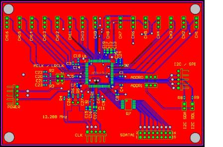
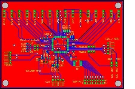
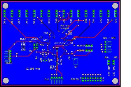
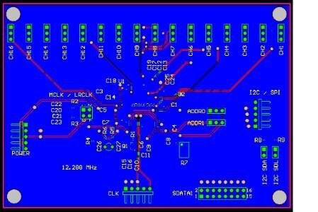
Looks good! I assume that this will be a 4-layer board, even though your screenshots only show the top and bottom. Is that correct?
With the high number of digital and analog I/O on a board like this, the performance will probably suffer if the board is only two layers.
For now I'm prototyping with a 2 layer as I can order a small batch (2 boards) so I can get the I2C/SPI control code in order for the DAC volume control. This way I can deal with the small glitches and errors on the programming side.
There's no replacement for a fully functional model that even if its got some "noise".
The chip and all most of the components can be recovered as I have my own Hot Air work station with the proper size TQFP nozzle and vacuum pick up tool. For me, this is part of the prototyping process and my local guy has to send out for 4 layer boards and charges and arm and a leg, however he can make me this prototype batch ( up to 3x 2-layer boards ) for under $25 which is not bad.
You really need to have four layers so you can have either two ground planes or a ground plane and a power plane. This is required to keep the impedance on the signal lines somewhat constant. The reason I say "somewhat" is because it is dependent on the trace width and the layer spacing. You are filling the top and bottom layers with copper for a ground plane and that will help but it is not a good as a proper plane below these planes. If you have a look at the data lines coming into the part. The interior data lines, 2-7, will not have a ground plane anywhere close to the signal trace. So you may end up having some clicks, pops and other digital "glitches" due to signal integrity problems. For the other signals it will be difficult to predict what the signal return paths will be without a ground or power plane.
The clock and data connectors should have ground on every other pin so the signal lines have ground on both sides. I think you are doing that on the SDATA connector but it is difficult to see if that is true. You should also do the same with the clock connector.
I also see a problem with C25. You have vias between the cap and the pins of the part. You need to change that so that the cap is the first thing the trace hits when it leaves the pins. Then after the cap you can then place the via there. This ensures that the cap is the most effective at keeping the noise out of the part and keeping any noise generated inside the part from causing issues elsewhere in your circuit. There may be other places that this happens. I see a few small vias near the pins so anywhere you need to filter the pins, the CM lines, the FILT pins or power pins, you need to make sure there are no vias between the filter caps and the pins. Sometimes you may not have a choice but usually I have found ways to do it. Having power and ground planes helps to give you options.
So when you are ready to build the production version I suggest you go to four layers. I understand the need to keep prototyping costs down!
Hi Dave,
Thanks again for stopping by and dropping a few words of wisdom.
A few changes were made :
- Input Pin Headers were replaced with UFL connectors
- 3 Larger Filter Caps ( 100uF ) were added in for DVDD, IOVDD and AVDD
- Separate Digital and Analog Supply connectors
As you mentioned about the caps, they are directly on the pins and the via's are there to tie the ground to the ground plane below.
And here's the end product
[IMG]http://i161.photobucket.com/albums/t221/adrculda/My%20DSP-DAC/DAC-GNDLayer-L2_zps76626c1a.jpg[/IMG]
It measures 74.04mm x 99.95mm
And here's the end product
First / Signal Layer
[IMG]http://i161.photobucket.com/albums/t221/adrculda/My%20DSP-DAC/DAC-SignalLayer_zpse466c4c8.jpg[/IMG]
Second / GND Layer
[IMG]http://i161.photobucket.com/albums/t221/adrculda/My%20DSP-DAC/DAC-GNDLayer_zps2dffe9ec.jpg[/IMG]
Third / Output Layer
[IMG]http://i161.photobucket.com/albums/t221/adrculda/My%20DSP-DAC/DAC-OutputLayer_zps98af916c.jpg[/IMG]
Fourth / Power Layer
[IMG]http://i161.photobucket.com/albums/t221/adrculda/My%20DSP-DAC/DAC-PowerLayer_zpsc84b7d81.jpg[/IMG]
Thanks for sharing.
I was wondering if you have any update or progress on the firmware side of your project.
Thanks,
David
Please log in to reply.