ADAU1452 pass transistor power dessipation
Hi Support Team,
I am assuming the DVDD current for ADAU1452 is to be maximum 40mA. Now when I need to calculate the power dissipation in the external pass transistor, I simply do (3.3 - 1.2) * 40mA. Now this comes to be around 84 mW. But if we see the recommended transistor as per datasheet, it is a high wattage transistor. Why is this? Is the current assumption wrong?
Thank you.
Regards,
Archana.
Audio Signal Processors
adau1452
SigmaDSP Audio Processors
Hello Archana,
I'm not sure where you got the number 40 mA, but that's not the expected maximum DVDD current for the ADAU1452. The datasheet will be available on the website in the next week or so, but for now, here are a few excerpts from the specification table.
At a temperature of 25 C...
Digital Current (DVDD)
Min
Typ
Max
Operation State
Maximum Program
350
415
mA
Typical Program
100
mA
Test program includes 16-channel I/O, 10-band EQ per channel, all ASRCs active
Minimal Program
85
mA
Test program includes 2-channel I/O, 10-band EQ per channel
Idle State
20
95
mA
Power applied, DSP not enabled
Reset State
20
95
mA
Power applied, held low
At an ambient temperature of up to 105 C...
Digital Current (DVDD)
Min
Typ
Max
Operation State
Maximum Program
500
690
mA
Typical Program
200
mA
Test program includes 16-channel I/O, 10-band EQ per channel, all ASRCs active
Minimal Program
160
mA
Test program includes 2-channel I/O, 10-band EQ per channel
Idle State
315
635
mA
Reset State
315
635
mA
So, as you can see, the absolute worst case current can be up to 690 mA.
In the section of the datasheet describing the regulator, we recommend the following transistor specs:
For proper operation, the linear regulator requires several external components. A PNP bipolar junction transistor acts as an external pass device to bring the higher IOVDD voltage down to the lower DVDD voltage, thus externally dissipating the power of the IC package. Ensure that the current gain of the transistor (β) is 200 or greater and the transistor is able to dissipate at least 1 W in the worst case. Place a 1 kΩ resistor between the transistor emitter and base to help stabilize the regulator for varying loads. This resistor placement also guarantees that current is always flowing into the VDRIVE pin, even for minimal regulator loads.
Hi BrettG,
Thank you. My bad, assumed wrong value. If I take the 690mA as worst current, the power dissipation calculation will be (3.3-1.2)*690mA = 1.5W (approx)
Is this the correct way to determine worst case PD in the external transistor? Do you see any other factors which can affect PD significantly.
Thank you.
Regards,
Archana.
Hi Archana,
It's not explained very well in those tables, but the 690 mA number is very much a result of "stress test" conditions and quite a bit of guard-banding. In a real world system, you shouldn't see DVDD current exceed 500 mA. However, it's always better to be safe and build in some extra safety margin. So, I agree with your calculation.
I believe our selected transistor for the evaluation board has a very significant safety margin. Here are its specs:
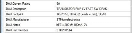
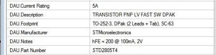


Above transistor specs will definitely help me to check the transistor selected for our design.
Thank you BrettG. This helped me a lot.
Thanks,
Archana.
Please log in to reply.