low swing clipping on ADAU1702 output
Hello, hope someone can help on this.
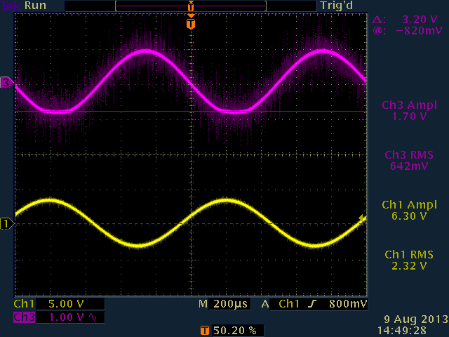
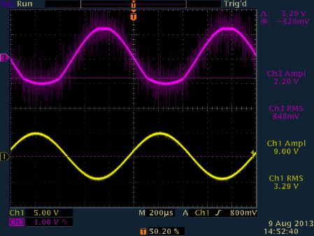
We have the sigma ADAU1702 running on our PCB's and we have two designs using this processor, The differences on the designs are larger amplifiers and more of them. The issue is the same on both. Our output signal at the DAC's is clipping at 0.9Vrms on the positive swing as it should, but only 0.65V on the negative swing. We have the mini eval board and we get a clean 0.9Vrms on it.
I have adjusted the input resistors and input seems to work as it should. The program is wired straight through for testing amps.
Atached are the output at 0.6Vrms and 0.8Vrms on the green traces. The other is the input.
Any insight would help. Thank you
Audio Signal Processors
adau1702
asymmetrical_clipping
dac_output_signal
SigmaDSP Audio Processors
adau1701
Show More
Hi enggeek,
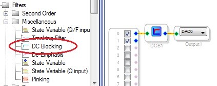
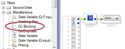
As a test, try inserting a DC Blocking filter into your signal flow as shown below:
As it turns out, the -1702's DACs do pass DC from their numeric inputs to their analog output pins, which can result in asymmetrical clipping -- see https://ez.analog.com/message/85908#85908
If adding the DC Blocking filter makes a difference, check your input circuitry for anything that might put a DC bias current into your ADC inputs (such as leaky coupling caps, or attempting to DC-couple the ADC inputs). The ADC inputs must be AC-coupled (or very carefully DC coupled from a source with the same quiescent level, about +1.5 V dc -- see https://ez.analog.com/message/42692#42692).
Best regards,
Bob
Hi George,
Bob's test is a valid one, the o'scope plots look like there is asymmetrical clipping, which would imply that you have some error in your reference voltage. Can you please post your schematic? We would be happy to review. If you are not comfortable posting your schematic on a public forum, please let me know and we can review your schematic in a private discussion.
Best regards,
Coleman
We will test the DC blocker, Thank you.
We do have a another module with a high pass filter I have not checked for this issue yet. It is out pounding on speakers testing the amplifiers. This output should block the DC input also.
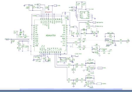
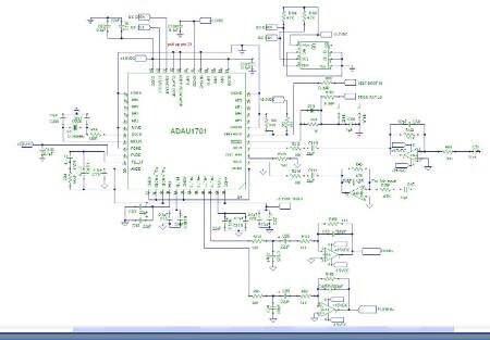
Here is the schematic: I will check the offsets at the input also.
Thank you.
Hi,
C110 and C111 are in with reverse polarity. You should find 1.5 V DC Common Mode reference voltage on the ADAU1701 side of the capacitor.
Your PLL Loop Filter should be directly connected to the PVDD (pin 34) reference, not to AVDD. This is a subtle issue, the Loop Filter should feedback right to its own power pin.
I do not recommend isolating GNDs. One single solid ground plane for the entire design will get you the best signal integrity with the lowest EMI transmission. There can be confusion in the design: AVDD is decoupled to AGND, but the PVDD is decoupled to DGND. The PLL and MCLK sections are part of the analog domain of the chip, decoupling them to DGND creates longer than needed current return paths. The IC itself has a ground ring, common to analog and digital. By isolating GNDs, you are forcing ground return currents, usually high frequency ones, through the ADAU1701. This will not help with stability and performance.
I2C pullups should be down in the 2k00 range, 4.7k might not be strong enough. You also might have other pullups on these lines on another page, in parallel with these. Please add PS decoupling to the EEPROM.
Best regards,
Coleman
I reversed the caps with no change. Thanks for pointing that out it is so easy to over look the obvious some times. That could be a future issue. In the previous design and DSP the bias came from the opamp. I will look into the grounding. This project changed DSP's several times. From internal to external codecs. The data sheet is a little lose on the analog and digital grounding, but I am seeing in the eval boards the common ground. The data sheet says the grounds "can be" connected together. It would have been nice to know they are connected together internally. The pull ups were changed. The 4.7K value was for a TI DSP part. Just not changed on my computer scheme for this revision.
These post are helping thank you,
George
Let me know if you have any more questions.
Best,
Coleman
Hi,
You may need to replace the coupling caps. Once they've been powered backwards, all bets are off.
Bob
Thanks Bob,
The reversed caps were new. I never saw a change in the bias voltage at that point. The first caps were 35V, so they never really saw the issue at 1.5V. Still waiting for a new program to test the DC blocking idea. The mini Eval was tested with straight through with no issue. You would think a 0.3V offset would be present on the input if it was the issue. I also grounded the digital to the analog in several points under the DSP. The High pass filter on the other module was attenuated to the point it could not put out a signal over 0.3V. It never reached the offset clipping to know if it was blocking any DC.
George
I have the DC blockers in the DSP program and the output is still asymmetrical clipping.
The program is a straight through connection. The DC blocker is on three of the outputs and I left one output just wire straight through. All the outputs have the same asymmetrical clipping.
Added note: For output 3 and 4 I have one inverted in the DSP going to a differentcial setup. I have the output 1 and 2 going single ended as in the scheme above. All four outputs have the same clipping at 0.65Vrms on the negative swing. The clipping was not inverted on output 4, so this seems to be an output issue.
Hope this triggers some ideas.
Thanks
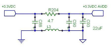
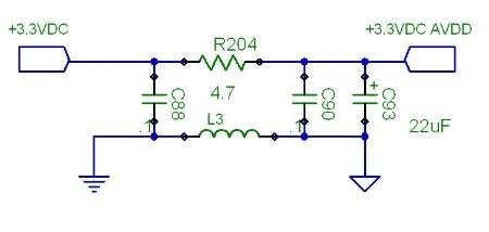
Found the reason for the offset output clipping:
The R204 had enough current across it to lower the AVDD to 3.0V. The bias is a fixed 1.5V, and there must be an inversion internal. This was cutting off the bottom of the wave in all outputs.
Thanks for the help I have updated a few other suggestions in our design.
Glad you tracked that down! Glad we could help with your review. Please let us know if you have any more questions.
BR,
Coleman
Please log in to reply.