EMI from SigmaDSP processors
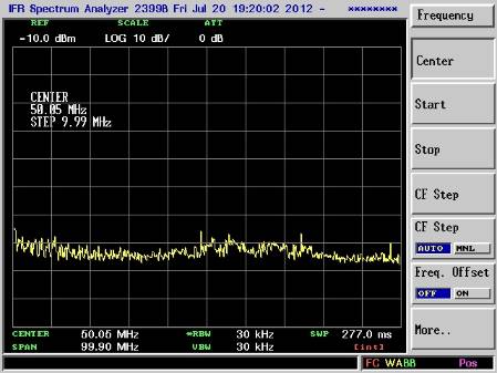
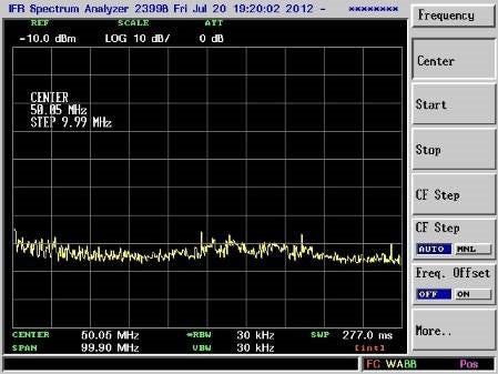
Our project is telephone-related so it needs FCC part 15 and 68 approval. We have received approval on other products that use only a PIC microcontroller, but 50 MIPS processors are new to us. Thus I did some very informal EMI measurements taken with a 6" wire draped on top of the circuitry in question, connected to a spectrum analyzer. All photos are 100 kHz -- 100 MHz. In this one, the wire is near a PIC microcontroller on our prototype board. As shown, there isn't much going on above the noise floor (about -85 dBm)
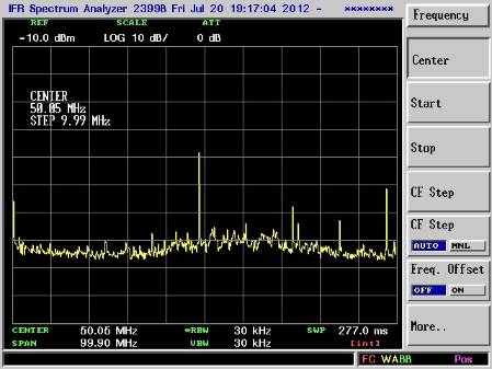
The next one shows when the wire is moved near the ADAU1701 on the same prototype. As seen, the largest spike is at the MIPS frequency (48 kHz x 1024).:
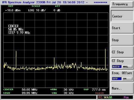
This prototype is a double-sided PCB with generous ground planes, however not necessarily following everything in the SigmaDSP PCB Layout Best Practices advice. For example, we placed the crystal right at the -1701 as we would do with a PIC, which of course is good -- but doing so traded off the closeness of perhaps more critical components. This and using 0805 caps for easier manufacturing, somewhat compromised our layout and resulting EMI performance. Compare this photo to the next one, showing the -1701 on its evaluation board as supplied by AD:
This shows something at the crystal frequency (~12 MHz), but is mostly quieter otherwise. Our next spin of this board will have 0603 caps; it will be interesting to see how this new layout will affect its EMI results. BTW -- In my opinion there's far too much EMI in the world. As a teenager I listened to all kinds of broadcast and amateur transmissions on a three-tube regenerative receiver. Now there's only buzz, regardless of gear.
*** Does anyone have experience with gaining FCC Part 15 Class B approval of a product containing Sigma DSP(s)? How did it go?
Audio Signal Processors
SigmaDSP Audio Processors
adau1701


I'm not very experienced in EMI measurement, but the best practices thread you're referring to is based on the ideal design rules that we have come up with for SigmaDSP systems, and I imagine that following it closely would keep your EMI pretty low.
Keep in mind that we had many tradeoffs to consider on our evaluation board designs as well. User-friendliness, sensible UI, legible silkscreening, minimizing board size (to minimize cost), and several other considerations came into play when creating the board. In saying all that, the point I'm trying to get across is that our boards are not ideal, optimized designs and they're not really intended to be used as reference designs for a real system.
It might be helpful to look at the high-frequency digital clock and data signals on the board for signs of ringing or overshoot, which could be mitigated by proper transmission line termination.
Happily we're basing our next board rev on the Best Practices thread, not the layout of the evaluation board (although I did examine it and found it followed that advice rather closely). I'll post the results when available..
Hi Brett,
Thanks again for your answer. It actually was the "correct" answer for EMI-proof design, but I had marked it merely "helpful" in order to keep my topic open for any EMI experience comments. None were forthcoming, however, and now the topic is "assumed answered" (I'm not sure how that happens). Regardless, I will go ahead and update my test results here when the second prototype is ready.
Bob
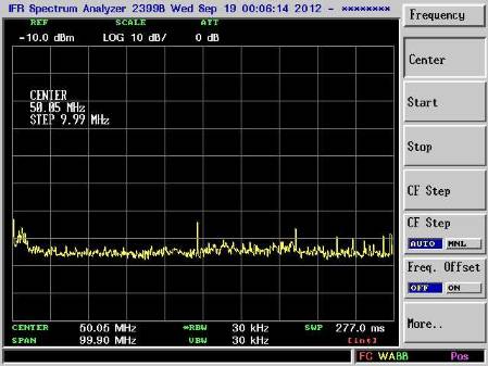
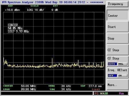
Here's the spectrum from the Rev B prototype, made more or less the same way as the previous photos:
The EMI level is lower now. This shows the benefits of more closely following the Best Practices advice.
Excellent. Thanks for updating us!
Hi Brett,
I'm happy to report that my company's product (the board described above in a small metal enclosure) recently passed FCC Part B conducted and radiated emissions tests. Thus with good layout practices, class-B performance is indeed quite achievable.
Bob
That is great news, Bob! It's great to know that a well-done 2-layer board can yield good results. And we look forward to hearing the results of your next tests with a board that follows our Best Practice recommendations.
BR,
Coleman
Thanks Coleman!
Now finally Mike and I can get to moving this product into production, and starting on the next one.
Bob
Please log in to reply.