Interfacing ADAU1701 with AD1955
Hi:
I am trying to send the I2S output from ADAU1701 acting as master to a DAC board built around the AD1955. Questions:
1. The ADAU1701 datasheet recommends on p18 that MP11 be used to derive MCLK. Now MP11 also serves the purpose of OUTPUT_BCLK when used for I2S. Therefore does this mean that I can connect MCLK and BCLK together?
2. The ADAU1701 operates at 3V3 and AD1955 at 5V. Is the ADG3304 a good choice to perform the voltage level translation between the two at these frequencies?
Thank you - Ram
Audio Signal Processors
Audio Products
Data Path Management
voltage_level_translation
i2s
Audio D/A Converters
Level Translators
SigmaDSP Audio Processors
ad1955
adg3304
adau1701
Show More
Hi,
I moved this question to the SigmaDSP Community. Please continue the discussion here.
Regards,
Colin.
Hi Ram,
1) Are you using a crystal with the ADAU1701, or an active oscillator? If you are using a crystal, I would recommend using a buffered version of OSCO to provide MCLK for the AD1955. If you are using an active oscillator, I would provide a second feed from it to the AD1955. You are correct that MP11 of the ADAU1701 should be used for BCLK; MCLK and BCLK will not be the same frequency, in most configurations. BCLK will be 64 × fs and MCLK will depend on your fs and register settings, usually 256 × fs.
2) The ADG3304 would be a good choice for translating 3.3 V serial audio into 5 V serial audio. 12.288 MHz (for fs = 48 kHz) has a duty cycle of 82 nS; the switching characteristics of the ADG3304 will be able to handle this well.
Regarsd,
Coleman
Hi Coleman,
Thanks for the insightful inputs.
1. I am using a 12.28 MHz crystal - pretty much ditto configuration as the ADAU1701 I2C config schematic in the datasheet, so that makes it 256xfs since I am using fs=48kHz.
Ahh - I now see these in a footnote in the AD1955 datasheet
- LRCLK NORMALLY OPERATES AT fS EXCEPT FOR DSP MODE, WHICH IS 2fS.
- BCLK FREQUENCY IS NORMALLY 64 LRCLK BUT MAY BE OPERATED IN BURST MODE
2. My primary intent is to use the AD1955 in the simplest possible config without a uC, so I am going by the default power-on parameters for the AD1955. if in this mode BCLK must be 64xfs, I conclude that the default hardware config in SigmaStudio must be altered for MP11 to "internal clock/4" for BCLK rather than "internal clock/16" which seems to be the default in SS.
3. The ADG3304 datasheet on page 16 says "To ensure correct operation of the ADG3304, the circuit that
drives the input of the ADG3304 channels should have an output impedance of less than or equal to 150 Ω and a minimum peak current driving capability of 36 mA." This threw me. Is this correct and if so could it work directly with the ADAU1701's outputs?
Thanks again!
Best - Ram
The BCLK output can be used as the MCLK output, but it's probably worth trying this first on the evaluation board to make sure the drive strength is sufficient to drive two input pins on the DAC.
We do not spec the output impedance of the ADAU1701's output drivers. I would expect, however, that the drivers are capable of providing sufficient drive strength to the ADG3304.
Thanks for the inputs Brett.
On looking at the AD1955 datasheet page 14 it appears that in the default mode without a uC the BCLK and MCLK inputs on the AD1955 can probably not be tied together because the default MCLK mode in Table II is 256fs.
So let me summarize what emerges; if something seems wrong or if additional changes are required, please point it out:
To send I2S from ADAU1701 to AD1955, with the AD1955 operating with SPI pins tied to DGND (no uC), do the following to the ADAU1701/SigmaStudio in the hardware configuration register control page: (ADAU1701 is operating at fs=48kHz and crystal of 256fs.)
1. Set MP10 to LRCLK and MP11 to BCLK respectively.
2. Choose an SDATA_OUT: set MP6, for example, to SDATA_OUT0.
3. In the "Serial Output 1" box, check "Master Mode".
4. Frame Sync Type - ensure "Frame Sync Freq" is at "Internal clock/1024". This makes LRCLK equal to fs=48kHz since the "internal clock" is 1024xfs.
5. BCLK Frequency - ensure it is set to "Internal clock/16"
6. Feed SDATA_OUT0, LRCLK and BCLK to a 3V3-5V translator; on the 5V side, connect them to the respective AD1955 inputs
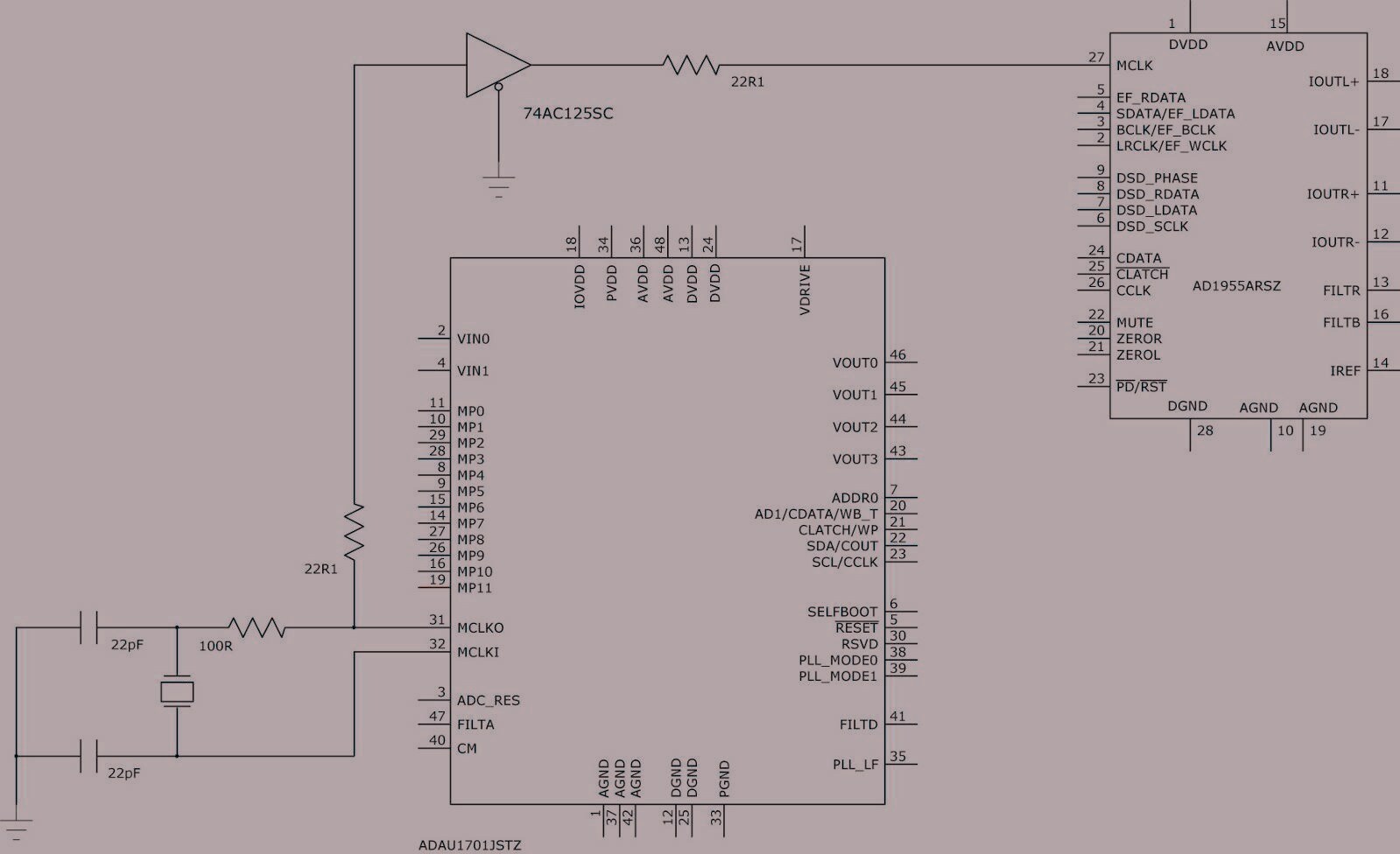
7. Buffer OSC0 on ADAU1701 and feed the signal to MCLK on the AD1955
- Ram
That sounds correct. In that case...
MCLK (ADAU1701) = 12.288 MHz
MCLK (AD1955) = 12.288 MHz
LRCLK = 48 kHz
BCLK = 3.072 MHz
If you take a buffered output of OSCO and feed it to the MCLK input on the AD1955, then everything should be in sync and work properly. The buffer is necessary because OSCO is only designed to drive a crystal and it will not have enough strength on its own to drive a trace to the AD1955's input pad.
Thank you for reviewing my spec Brett.
Meanwhile I have chosen the ADG3308 instead of the ADG3304 because the A-side Input High Voltage (Min) spec for the 3308 is 0.65xVcca as opposed to Vcca-0.4 for the ADG3304. This means that with the ADG3304 the ADAU1701 needs to output 2.9V for it to be recognized as logic 1 by the ADG3304 but only 2.15V for it to be recognized as logic 1 by the ADG3308. In reality the ADAU1701 outputs closer to 2.4V so it should, going by the specs, not work with the ADG3304. Hmmm.
I will shortly implement a 3V3-5V translation-plus-MCLK-buffering scheme using a ADG3308, and will post the outcome if successful.
Best - Ram
Hello BrettG,
Could you explain more about " take a buffered output of OSCO and feed it to the MCLK input on the AD1955"
Could you draw a schematic of it?
Sorry if my question is fool
Thanks in advance!
Hello Huy,
Please find the attached schematic that shows how you should connect the MCLKO/OSCO pin to the AD1955 MCLK Input. I have added 22R1 resistors to improve the signal integrity.
Best regards,
Coleman

Thank you very much, this is what i am looking for.
Apologies for the bump.
Does there need to be a level shifter from the ADAU1701's 3.3V to the AD1955's 5V when using this buffer?
Does the supply voltage of the buffer matter here?
Hi Alex,
I answered the level-shifter question in your other post on this subject. I would recommend that you follow this schematic for your OSCO to AD1955 MCLK connection.
Best,
Coleman
Please log in to reply.