Adding additional GPIO ADC functionality
I have a general question regarding the SigmaDSP GPIO ports which came up as I was thinking of new designs. In the ADAU1701 we have 12 GPIO ports but only 4 of them can be configured as ADC inputs. If I had a design that required parameter control using 8 analog, linear pots as the control sources, what would be the best way to add the additional 4 ADC functionality? I would ideally like to stay away from using rotary encoders or an external micro, although I might reconsider if it's the only option.
Thank you!
Audio Signal Processors
SigmaDSP Audio Processors
adau1701
At the moment, I can't think of a reasonably simple way to manage to do this. I had imagined some kind of method that would use GPIOs to toggle analog switches that would allow you to multiplex several pots on to one aux ADC pin, but that would require complex, custom code.
This is pretty much what I figured.
Now, what if I have a PIC micro available? Is there a way in which the GPIO pins can be configured to accept a binary signal to switch various externally controllable blocks within SigmaStudio? Essentially I have an existing, fully analog system which has level control, tone controls, limiter controls, etc., which are all currently controlled with potentiometers. I need to keep the potentiometer interface as it is, but want to do all of the signal processing inside of a Sigma DSP.
Thanks!
I think you would need some kind of ADC that would take in the potentiometer and then output some digitized representation of it (PCM, for example), and then have the PIC translate that into a parameter that can be written via SPI/I2C to the corresponding register in the SigmaDSP.
In the SigmaDSP program, you would just create a DC constant source in the schematic, which would then be assigned to a parameter RAM location by the compiler. The PIC would then need to update that parameter each time the potentiometer is polled.
Thanks for your help so far Brett.
In looking over this problem, and evaluating our other requirements for this system, I have decided the best way to go would be to use two ADAU1446 DSPs and a single AD1938 CODEC. This would give us the extra processing horsepower we are going to require, and gives us the number of ADC GPIOs we need. Could you let me know if this would work?
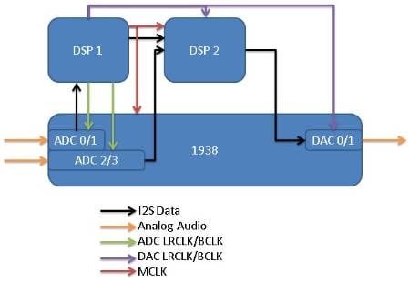
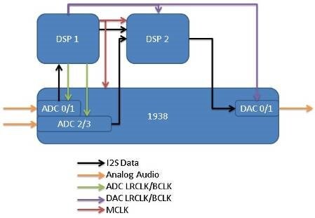
Two A/D channels of the AD1938 are input to DSP1. A mono digital bit-stream is output from DSP1 and input to DSP2. DSP2 also has the other two A/D channels of the AD1938 as inputs. These three channels will then be combined and conditioned within DSP2 and then a stereo output is produced using two of the D/As in the AD1938. My only concern is clocking between the signals from DSP1, DSP2, and the CODEC. Is there an example somewhere showing a system with mutiple Sigma DSPs?
Thanks!
Hi audiolab1,
This setup would work. I would suggest using the same MCLK source for all three ICs in the system. The de-jitter circuitry in the DSPs and CODEC will handle any jitter that is introduced into the system because of the slight differences in each IC's PLL. It might make sense to have one DSP act as a master, and the other devices act as slaves.
Here's a simple diagram of how that would work.
Hi Brett,
I have done up a basic schematic showing the interconnection between an AD1938 codec and two ADAU1446 DSPs. A copy is attached to this post. Here is how I have things set up:
AD1938
Set as slave
MCLKI set to EXT_CLK from CLKOUT of DSP1
ADAU1446 (DSP1)
Set as master clock
Provides CLKOUT for AD1938 and DSP2
PLLx set to mode 010, 256xfs
CLKMODEx set to mode 01 (buffered oscillator output)
ADAU1446 (DSP2)
Set as slave using CLKOUT from DSP1
PLLx set to mode 010
CLKMODEx set to 00 (disabled)
Now what I want to do is send the data from IN1 and IN2 of the codec to DSP1 and IN3 and IN4 to DSP2. The audio data from DSP1 is then sent to DSP2. Finally, a stereo output from DSP2 is sent to codec output OL1/OR1.
ASDATA1 (IN1 and IN2) from the codec is sent to SDATA_IN0 of DSP1.
ALRCLK from the codec is connected to LRCLK0 of DSP1.
ABCLK from the codec is connected to BCLK0 of DSP1.
ASDATA2 (IN3 and IN4) from the codec is sent to SDATA_IN0 of DSP2.
LRCLK9 of DSP1 is connected to LRCLK0 of DSP2.
BCLK9 of DSP1 is connected to BCLK0 of DSP2.
SDATA_OUT0 of DSP1 is connected to SDATA_IN1 of DSP2.
Finally, SDATA_OUT0 and SDATA_OUT1 are sent to DSDATA1 and DSDATA2 of the codec and LRCLK9 and BCLK9 form DSP2 are connected to DLRCLK and DBCLK of the codec.
I pretty sure the data lines I have proposed are correct, but I am not positive that I have the various clocks connected properly. I would appreciate it if you could have a look and let me know if I have anything routed incorrectly.
Thanks!
Hi Audiolab1,
I have looked at your schematic and have a few suggestions:
For Codec1, I would recommend that you tie the unused DSDATAx pins to ground.
In the case of your Master/Slave mode and MCLK jumpers, I would recommend using a 3-pin jumper, instead of 2 2-pin jumpers. Using a 3-pin jumper will make the selection exclusive, so that you cannot short DVDD to GND, or the CLKOUT signal to your crystal.
I would add some line termination to your clock and data lines, in the form of series resistors. 33.2 ohms would be a good starting value, and you can look at the integrity of the signals on the board and tweak as necessary.
Where is the FILTR net going? You need to be very careful about the loading of this pin, the source is high impedance and . Also, I would increase the value of the CM and FILTR decoupling capacitors to 47 uF; the CM will help with crosstalk between channels and the FILTR will help with noise level.
Do you have a pulldown on your reset line in another place in the schematic? It is best practice to pull this line low and assert it high at the appropriate time.
You are not showing any power connections in this drawing. I hope that you are going to apply HF decoupling to each pin, with a 10 uF reservoir near each device.
I would consider using LRCLK0A and BCLK0A to drive the CLK0 ports of both devices, so that the timing between LRCLK9A and SDATA_IN0B is not an issue. The ALRCLK and ABCLK ports of the AD1938 should be OK to drive both CLK0 input ports on the ADAU1446s.
Otherwise, your signal and clock routing looks good.
Regards,
Coleman
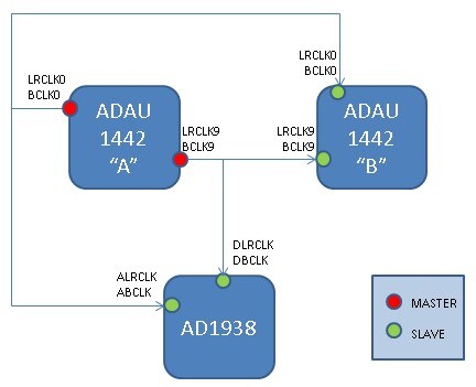
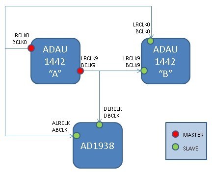
I would suggest this clocking scheme for the serial port clocks:
The ADAU1446 "A" device is the master on all of its serial ports. The ADAU1446 "B" device and the AD1938 are slaves on all serial ports. This will guarantee that everything is synchronous.
The data connections and the master clock routing looks OK.
Thank you Coleman and Brett.
I have updated the earlier schematic with your suggestions. Coleman, I have added the suggested termination resistors at the source end of all data and clock lines, as this is what I remember as being the correct place for them. The FILTR net is used as the voltage reference (non-inverting inputs) of my input op-amps that are performing single-ended to differential conversion. I have changed the FILTR and CM decoupling caps to 47uF as suggested. Please let me know if I have implemented the revised clocking scheme correctly.
Thanks!
Clocking and data looks OK!
May I ask why you are putting crystals on all three devices and then using a jumper to select between the crystal or the CLKOUT signal for the codec and DSP B? I'm just curious. I guess that might give you a good way to test the ASRCs if you wanted to try those out, but other than that, it seems unnecessary. In normal operating conditions, I expect you'll choose to use the CLKOUT signal coming from DSP A to clock DSP B and the codec.
Bumping this topic as I now have a board prototyped to the above schematic. What should the level of the CLKOUT signal be when CLKMODE is set to "buffered oscillator"? I am only seeing a peak to peak voltage of 400mV before the 33R2 resistor (directly out of the DSP) and 100mV peak to peak after. It seems something is wrong here as the CODEC and the second DSP that are slaved to the first DSP are not operating. The CODEC is set as SLAVE and the system is set up for 96kHz. PLL mode is set to 256 x fs,normal. I originally programmed only DSP1 in SigmaStudio and then checked for operation of the CODEC. Thinking that maybe DSP2 must also be setup, I tried to program it but got a COM failure...something I have seen before if the DSP does not see a master clock. Any ideas what might be going on? I can post my SigmaStudio project if it would help.
Thanks again for your help!
False alarm!
I found a small short between DGND and the MCLKI on the Codec. Once corrected everything is working perfectly. Thank you again Coleman and Brett for your assistance with this project!
Thanks for the update! I was scratching my head with this one. I'm glad it was a simple hardware fix.
Please log in to reply.