SPORT output timing after register setting
Dear support team,
My customer wants to know the delay time of output BCLK and FS of SPORT after register setting.
(Set the register -> (delay time) ->starting BCLK and FS output)
Background:
They connected SPORT out to D-AMP.
BCLK and FS of SPORT is operating clock for D-AMP.
So,microcomputer can't access to the D-AMP before output BCLK and FS.
So,they wants to know the delay time.
Could you tell me about it,please?
Best regards,
Takehiro Yabune
adau1401a
Audio Signal Processors
SigmaDSP Audio Processors
Hi Yabune-san,
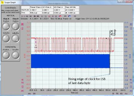
There is no delay between the register write and the enabling/disabling of the clocks. You can see from the examples below that the clocks will be enabled before the I2C write is completed.
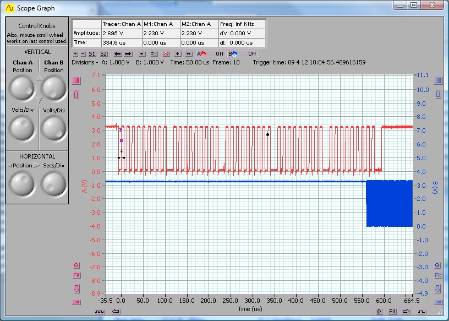
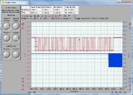
Clock enable:
(Write 0xA400 to address 0xE000)
The red signal is the SCL (I2C clock) line.
The blue signal is the BCLK line.
I write 5 bytes: Chip address, subaddress 0, subaddress 1, data 0, data 1.
The bits that enable the clock are in the 4th byte, data 0.
During the 5th byte, the BCLK signal starts.
So, the BCLK signal starts before the end of the I2C write.
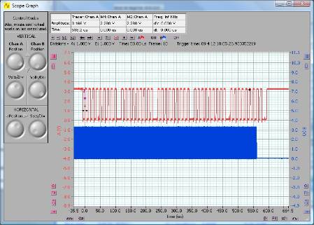
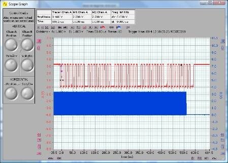
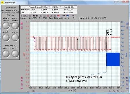
Here is an example of disabling the clock:
(Write 0x2400 to address 0xE000)
Again, I write 5 bytes: Chip address, subaddress 0, subaddress 1, data 0, data 1.
The bits that disable the clock are in the 4th byte, data 0.
During the 5th byte, the BCLK signal disables.
So, the BCLK signal disables before the end of the I2C write.
It looks like the total delay between the data latching into the register and the actual start of the BCLK signal is about 100 microseconds, or 0.1 ms. This should be independent of the data rate on the control port.
Best Regards,
Brett
Thank you very much Brett-san!!
Best regards,
Takehiro Yabune
Dear Brett-san,
I got a feed back from customer about your answer.
Q1.
They want to know the delay time which is counted by architecture.(not actual measurement).
Could you tell me about it,please?
They use SPI port to control ADAU1401A.
Q2.
In your answer, you wrote "write 0xA400 to address 0xE000).
But, 0xE000 is not in memory map of ADAU1401A.
What is correct address?
Best regards,
Takehiro Yabune
Hi Yabune-san,
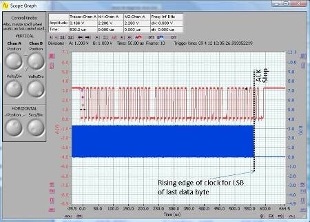
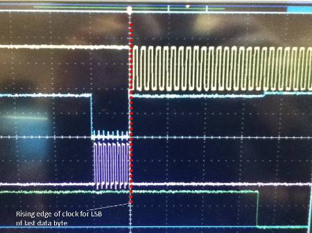
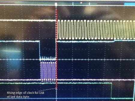
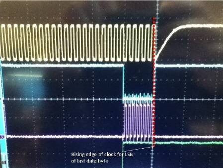
The answer to your first question is zero. There is zero delay between the end of an I2C or SPI write and the clock turning on or off. On the last edge of the clock (aligning with the LSB of the last data byte), the data is latched in parallel into the register and the clock immediately turns on or off, with zero delay.
(On my earlier response, I was confused because on I2C there is an acknowledge and then a stop condition, which makes it look like the clock turns on/off before the end of the write. In fact, the clock turns on/off exactly at the end of the write.)
This timing is determined by the control port - it is completely independent of the system MCLK or the serial clock rate on the control port.
For I2C (tested at 400 kHz):
For SPI (tested from 1 MHz up to 4 MHz):
With regards to your second question... I accidentally posted the register settings for the ADAU144x instead of the ADAU1401A.
The proper register is 0x081E. The data is:
0x08 0x00 for turning on the clocks, and...
0x00 0x00 for turning off the clocks.


Please log in to reply.