DC Couple Audio ADC input?
Odd question: Can the capacitor usually connected in series to the (audio) ADC be safely omitted to allow DC-coupled input? If so, is there any special treatment due to the internal biasing scheme used? (In particular the ADAU1701.) The input would be DC-20kHz or so.
Audio Signal Processors
SigmaDSP Audio Processors
adau1701
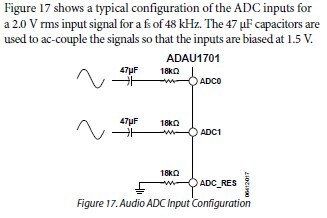
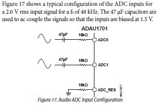
The ADAU1701 uses a switched-capacitor input, so the input signal is based on fluctuating current, rather than fluctuating voltage. The internal biasing attempts to keep the input node at exactly 1.5 V. The input resistor effectively acts as a current-to-voltage converter.
If you remove the AC-coupling capacitor and instead input a DC-coupled signal centered at 1.5 V, there is a chance that it will not be centered at exactly 1.5 V (in other words, there will be a small offset). This causes a constant current on the input, which then limits the dynamic range of the ADC.
This effectively raises the noise floor of the ADC, weakening its signal-to-noise performance.
So, while it's possible to do this, I would recommend strongly against it because of the resulting drop in audio quality.
Here is a diagram for reference.
Thanks, Brett.
I can tolerate reduced fidelity as long as the accuracy of DC (and AC) is still there. I should have stated that it's a utility/monitoring reference, where we want to know the full magnitude of a signal (DC+AC), with better resolution than the 8-bit utility lines allow. (This isn't just to save us a cap. We want to make use of the DC component.)
From that perspective, the undesirable offset you speak of would just be the DC part of our input signal, wouldn't it? We could scale the input to 0-2.8V (or so), DC+AC, and feed it right in. Or would the internal biasing cause errors or other odd behavior?
Hi Joe,
Is there any chance you would consider routing the DC component of the signal to the auxiliary ADC and the AC component to the audio ADCs? That would allow you to combine them in software to get the result you need. You'd keep the performance on the AC side and have a slightly reduced precision on the DC side.
I think I wouldn't recommend routing any single-ended signal to the ADCs directly unless it is centered at 1.5 V. Any other offset would create a DC offset that could cause some problems. Keep in mind that the ADC "wants" to see 1.5 V. If your signal was at 1.4 V, that would be a -0.1 V offset, and if it was at 1.6 V, that would be a +0.1 V offset. That's probably not a big deal, but I can imagine that at more extreme offsets like +1.0 V or -1.0 V, there could be some very odd behavior.
Since we characterize and test these ADCs using the recommended circuit in the datasheet, I'm not sure exactly how they would react in this scenario.
Thanks. I did consider sending the DC to the aux inputs but it sacrifices a lot of precision, so I wanted to avoid it. Plus we're short on aux channels.
I understand the ADC "wants" 1.5V, but I'm not really understanding how a large offset would be detrimental (how badly does it "want" 1.5V? ). Other than it being a different configuration to what is typically done, is there any specific reason to believe that odd, inaccurate, or harmful results would result? I haven't seen an issue sending DC into other switched-cap DACs; is there anything special or unusual about the ones inside the ADAU1701?
(Also do you know off-hand what the useful sample rate is for the aux channels? Is it the full system rate / 4?)
Hi Joe,
The two design engineers who could best answer this question are out of the office this week. I'll have to put you on hold until they come back.
My gut feeling is that you're just going to end up with a large DC current on the ADC that wasn't really meant to be there. While it's very unlikely that this would damage the chip in any way, I have a feeling that it would hinder the performance of the ADC in terms of noise and distortion. I'll try to confirm with the design engineers soon.
Thank you Brett.
I look forward to hearing their comments. I suspect we could tolerate a modest hit to noise/THD, as long as it was only on that ADC channel (leaving the other unaffected). More importantly, of course, since we can only test a small number ourselves we'd want to be sure the behavior was at least going to be consistent between chips, and reliable in a product design.
What would the range of the DC component be? That would be a good data point for my discussion with the designers.
Theoretically I'd like to use essentially the full scale of the A/D with DC or AC (or a combination), much like in typical A/D's. My intent was to scale my signal of interest to the range appropriate for the A/D.
Did you ever hear anything definitive about this?
Sorry, I forgot to post the response. Apparently my understanding of the inner workings of the ADC was a little bit off.
Here's the response from a designer:
The input is not switched-cap, it looks just like an op-amp.
Removing the 47uF capacitor would cause some DC offset, but this doesn’t increase the noise, only the DC term. If you have a lot of DC offset then the ADC might clip a little asymmetrically on a sine wave.
So, I guess that means you are free to go ahead with your plan!
Perfect, thanks.
Please log in to reply.