ADAU1442 Serial Audio Port question
Hi;
I am using an ADAU1442 in TDM4 mode (not packed) and have several questions:
1) Do settings of Serial Input Port Modes [9:3] (BCK pol, LRCK pol,... I2S, bit delay, Left Just...) affect TDM operation?
If so which bits impact TDM4 operation.
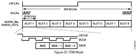
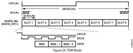
2) In TDM4 operation does the position of the LRCK rising edge matter? Note that in figure 25 it does ot align with the Slot 4/5 boundry.
3) I want to use an asynchronous BCLK in TDM4 mode which is greater than 128*LRCK. Can I just put out LRCK down edge, and 128 BCK cycles with 128 data bits (24 bits active 8 bits fill 24 bits active 8 bits fill 24 bits active 8 bits fill..) untill 4 channels of data are input, (or 129 cycles if I2S/Left Justified cannot be selected see 1) above). Or should I output 64 bits of data, wait for LRCK up edge then another 64 bits of data.
I find the data sheet inadequate in this area, is there a better reference?
Thanks in advance for any answer.
Brian
Audio Signal Processors
adau1442
SigmaDSP Audio Processors
Hi Brian,
Lots of questions here. I will have to get back to you about this on Monday.
1) Do settings of Serial Input Port Modes [9:3] (BCK pol, LRCK pol,... I2S, bit delay, Left Just...) affect TDM operation?
If so which bits impact TDM4 operation.
Hi Brian. All of these bits affect the operation. The serial ports are completely orthogonal and totally programmable. Each bit does exactly what it says it does independently of the other bits in the register. The serial ports are made to be so flexible because different codecs and serial interfaces on other ICs have a variety of ways in which they handle the data. We give you all of the options for setting up the ports the way that your target interfaces need to handle the data. Here are some examples.
First, the default settings of the serial port in TDM4 mode.
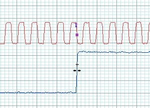
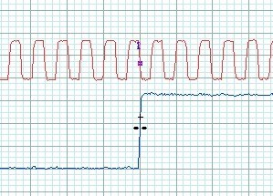
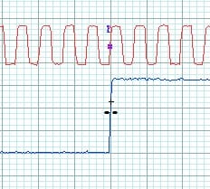
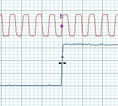
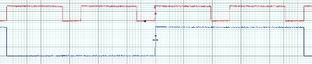
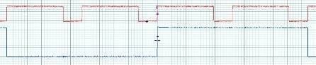
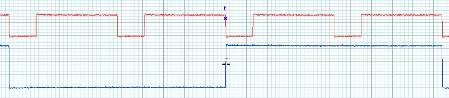
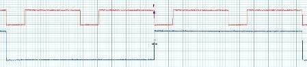
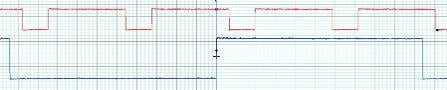
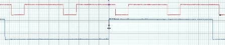
The red line is data, and blue line is LRCLK. Here you can see four data channels (all outputting all zeros for clarity) vs the LRCLK. Note that the start of each data edge is 1 BCLK delayed from the edge of the LRCLK.
Now, I change the LRCLK polarity.
As expected, the LRCLK basically flips upside down relative to the 4 data channels. (This would be easier to see if each channel had individual data that was more identifiable).
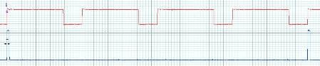
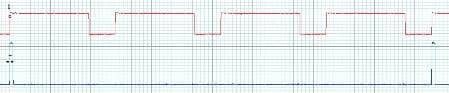
Now I'll do the same thing with BCLK polarity. The red line in the next two screenshots is BCLK. Here's negative polarity:
And here's positive polarity:
Now I'll start changing the MSB position. Here's Left-Justified (delay by 0).
Now you see the data channels line up with the LRCLK edges.
Here's delay by 8 mode. You can see that the LSB of the last channel lines up with the LRCLK edge.
Here's delay by 12.
Note that the last edge of the last channel actually overlaps the edge of the LRCLK. Whether or not your target interface can handle that is up to you - we're simply allowing you the option of doing this, even though it's very uncommon.
Even more uncommon would be a delay by 16 mode:
Here, there's a huge overlap of the last data channel and the start of the next frame. Again, whether or not this works depends on what target IC you're using. We're just trying to make it as flexible as possible. The only thing you can't really change is the number of bit clocks per channel. That's fixed at 32.
Lastly, here's an example of pulse mode on LRCLK.
You can see that the LRCLK now changes to a single pulse.
So, as you can see, every bit setting matters on the serial ports. You need to set up the bits in the way that your target IC expects to send or receive the data.
2) In TDM4 operation does the position of the LRCK rising edge matter? Note that in figure 25 it does ot align with the Slot 4/5 boundry.
That depends entirely on your target IC. If your target IC wants the LRCLK rising edge to align with the first data slot, for example, you need to flip the LRCLK polarity and set the MSB position to delay by 0 mode. The datasheet figures are just examples of possible configurations; each serial ports has over six hundred possible mode permutations, if you can believe it, so it would be a very long datasheet if we showed them all!
3) I want to use an asynchronous BCLK in TDM4 mode which is greater than 128*LRCK. Can I just put out LRCK down edge, and 128 BCK cycles with 128 data bits (24 bits active 8 bits fill 24 bits active 8 bits fill 24 bits active 8 bits fill..) untill 4 channels of data are input, (or 129 cycles if I2S/Left Justified cannot be selected see 1) above). Or should I output 64 bits of data, wait for LRCK up edge then another 64 bits of data.
I believe the serial ports just use a counter starting on the starting LRCLK edge for the frame. If the number of BCLKs exceeds the expected amount, the excess data slots are un-used. I haven't actually tried this out, but based on what the designers tell me about how the chip works, it's just a counter that will stop at 128 and will not reset itself until the next LRCLK edge, so extra cycles should not cause problems.
I know that for a fact in LRCLK pulse mode. In 50/50 wave mode it might re-sync itself on the edge halfway through the frame, so that might cause problems in your case. Are you able to hook those signals up to the evaluation board and give it a try?


















Thanks Brent,
The only issue left unresolved is why figure 25 shows LRCK down edge not
aligned with the Slot 4/5 boundary. The two clock modes are pulse or
50/50. Since it is not pulse then 50/50 should align with Slot 4/5
boundary. My best guess is that the only edge of LRCLK that matters is the
SOF edge and 128 bits follow that. Opposite edge of LRCLK is ignored. The
other possibility is that the opposite edge is relevant and I should clock
out 64 bits, wait for the LRCLK opposite edge than clock out another 64
bits. Remember I am clocking out 48 ksps data at 24MHz.
It seems like ADI could give a precise answer to this aspect, as it matters
to me.
Thanks
Brian
On Tue, May 3, 2011 at 11:31 AM, BrettG <
I hadn't looked at Figure 25 when I wrote my earlier reply. Looking at it now, I can see that this figure is flawed. The LRCLK duty cycle is not 50% in that figure, which leads me to believe that the illustrator just made a mistake. It should instead look like this:
I'll ask the serial port designer about your specific question. Due to the time zone difference between the US and Europe, I don't expect an answer before tomorrow.
I just sent the email and received an out of office response. The designer is on vacation, returning May 11th. I will ask around to some other colleagues, but I may not have a definitive answer before next Thursday.
Thanks Bret, for your help. I'm sure you are wondering why I do not try
both assumptions and answer my own question. My problem is the firmware
developers are in Belarus and I am trying to tell them what to do... I
think the 128-bits clocked in in TDM4 mode way of describing this implies
that the opposite edge of LRCLK does not matter but then why say 50%????.
The only mode that is clearly defined is the pulse mode but I do not want to
change my documentation..
I will assume the edge does not matter for now and await your response.
Thanks;
Brian
On Wed, May 4, 2011 at 1:53 PM, BrettG <analog@sgaur.hosted.jivesoftware.com
Brian, here is the response from the designer:
Yes, in theory this should work fine. As you mentioned, everything gets synchronized to lrclk, so the extra bit clock(s) will just be ignored.
My disclaimer is that we never actually tested this because it's not a standard operating mode for codecs and other I2S ports, so the only way to be 100% sure is to test it on the customer's hardware. Note that this should work for both wave and pulse mode for LRCLK.
Hi Brett;
Thanks for the response but ... My question is whether the opposite edge of LRCLK matters. Should I clock out 64 bits after falling edge of LRCLK then wait for rising edge and clock in another 64 bits or clock out 128 bits after the falling edge of LRCLK. The extra clock cycles obviously matter in that case as either the ADAU1442 will clock in bits for slots 3/4 immediately after 1/2 or after the rising edge of LRCLK.
The data sheet is inconsistent and it seems I should be able to get a concise answer.
From my understanding of the designer's response, only the beginning of the frame matters; after that, it's all counting. The clock edge in the center of the frame will not impact anything.
Basically, the LRCLK edge signalling the start of the frame makes the serial port wait for the next valid BCLK edge. When that arrives, the serial port starts outputting data in alignment with the BCLK. There is an internal counter here that keeps incrementing until it reaches 128. Then, the serial port effectively goes in to "wait mode" again until the next LRCLK edge signalling the start of the next frame arrives.
Brett;
Just reporting back. I instructed the firmware developers to ignore opposite edge of LRCLK and everything seems to work fine. One edge to start frame then clock data with BCLK to fill entire frame.
Thanks
Brian
Great, thanks for reporting back!
Please log in to reply.