ADAU1445 clock routing.
I've got an I2S stream, with it's respective clocks incoming @ IN0 that is slaved to BCLK1/LRCLK1.
Similarly I've got 4 I2S data streams being output on OUT0-3. I have the same BCLK and LRCLK that the input I2S data stream is clocked to, connected up to and set as a slave on BCLK10 and LRCLK10, on the output clock domain, domain 10.
If I set OUT0-3 as slaves so that they are clocked to output domain 10 then I get an I2S data stream present on the outputs. Likewise if I set them as a slave to the wrong clock domain the I2S data outputs stop running, so the chip is obviously clocking the data streams to the correct domain. However I was under the impression that if all the output domains were set up as slaves to domain 10, that the clock pairs (BCLK/LRCLK) associated with those domains (pairs 3 - 11) would actually buffer and output those clocks on their respective pins. Is this the case?
Currently when all the output clock domains are set as a slave to domain 10, none of the corresponding output clock pairs do anything. There are no clocks on the output pairs.
Obviously this is not what I was expecting. I expected the output domain to clock the outgoing I2S data stream to the domain it is slaved to and then buffer and output the clocks present at that slave domain on the correct pair of output pins.
I have the system working (and working very well I might add) by manually (literally soldering wires) feeding the BCLK and LRCLK into my DACs.
Is there any way to get the clock pairs to buffer and output the clocks on the clock domain that they are slaved to?
Audio Signal Processors
adau1445
SigmaDSP Audio Processors
MadMatt wrote:
However I was under the impression that if all the output domains were set up as slaves to domain 10, that the clock pairs (BCLK/LRCLK) associated with those domains (pairs 3 - 11) would actually buffer and output those clocks on their respective pins. Is this the case?
When a serial port is in slave mode, there is absolutely no connection between it and the clock domain (LRCLK/BCLK pin pair) of the same number. It only has a connection to the slave clock domain specified in its register setting. So, if I set serial output port 5 (SDATA_OUT5) to be a slave to clock domain 8 (LRCLK/BCLK8), then there is no connection at all between serial output port 5 and clock domain 8.
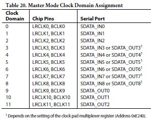
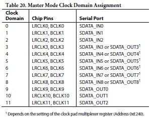
However, in master mode, there is a direct connection between the serial port and the clock domain. That relationship is shown in the datasheet:
Assuming the serial port is in master mode, you can enable its output clocks. If and only if those conditions are true, you'll see clocks coming out of the respective clock domain's LRCLK/BCLK pin pair.
The reason for this is because the internal clock generation buffers do not have any option to be connected to a slave clock input buffer. This means, effectively, that the ADAU144x cannot generate any clocks other than fs,NORMAL, fs,DUAL, or fs,QUAD (48 kHz, 96 kHz, and 192 kHz, respectively). In other words, the ADAU144x cannot be used as a buffer for slave clocks.
Thank you for your reply, it really helped to fill in the one missing link I had with regards to this and now it all makes sense!
Please log in to reply.