ADAU1452 EVM DAC and ADC clock domain
Hello everyone.
On page 39 from EVAL-ADAU1452REVBZ user guide said us that ADAU1452 is DAC CLOCK MASTER and ADC CLOCK MASTER. In EVM SDATA_OUT0, SDATA_OUT1, SDATA_OUT2 and SDATA_OUT3 runs with LRCLK_OUT0/BCLK_OUT0. Also SDATA_IN0 and SDATA_IN1 runs with LRCLK_OUT1/BCLK_OUT1.
But the datasheet said us that each clock domain corresponds to exactly one serial data pin, one frame clock pin, and one bit clock pin.
I got confused because the EVM uses MASTER CLOCK where different serial data pin uses the same domain clock.
Could anyone explain me???
Audio Signal Processors
adau1452
Datasheet/Specs
SigmaDSP Audio Processors
Hella francismariano,
francismariano said:
In EVM SDATA_OUT0, SDATA_OUT1, SDATA_OUT2 and SDATA_OUT3 runs with LRCLK_OUT0/BCLK_OUT0.
I'm not sure how you came to this conclusion. In a new SigmaStudio project every port (input and output) acts as a master in default so the hardware. Every port (both input and output ports) has its own Master BCLK and LRCLK. You can use every port as a master Or You can slave any port to one of the ports which should be the master but not between input and output ports(internally).
For ex, you could externally jumper the LRCLK_0 and BCLK_0 pins over to either serial output port 1 or 2 and then set serial port 3 to be a slave off of one of those clock domains(serial output port 1 or 2).
There are few things to understand here about the serial port clock slaving.
This thread would help you to understand this more : ADAU1452 SDATA_OUT3 SLAVE to CLK DOMAIN 0 does not work - Q&A - SigmaDSP Processors and SigmaStudio Development Tool - EngineerZone (analog.com)
francismariano said:
Also SDATA_IN0 and SDATA_IN1 runs with LRCLK_OUT1/BCLK_OUT1.
There is no internal connections between serial input and serial output ports. However, you can use the clocks externally by using a jumper cable if it's required and proper config must be done in the serial port register page.
francismariano said:
In EVM SDATA_OUT0, SDATA_OUT1, SDATA_OUT2 and SDATA_OUT3 runs with LRCLK_OUT0/BCLK_OUT0.
This is possible when you configure serial output port 0 as a master (BCLK,LRCLK) and slave every other serial output ports (serial output port 1, serial output port 2, serial output port 3) to serial output port 0. But As I said above, there are few things to note here. Please follow the above mentioned link.
francismariano said:
I got confused because the EVM uses MASTER CLOCK where different serial data pin uses the same domain clock
If you are stuck anywhere in your project then please send your project with little bit info of what you want to do.
Regards,
Harish
Hello francismariano,
I think I understand your confusion.
francismariano said:
On page 39 from EVAL-ADAU1452REVBZ user guide said us that ADAU1452 is DAC CLOCK MASTER and ADC CLOCK MASTER. In EVM SDATA_OUT0, SDATA_OUT1, SDATA_OUT2 and SDATA_OUT3 runs with LRCLK_OUT0/BCLK_OUT0. Also SDATA_IN0 and SDATA_IN1 runs with LRCLK_OUT1/BCLK_OUT1.
On the eval board there is one codec. It has four ADCs and 8 DACs. It just needs one set of clocks to run both the ADC or the DAC sides of the part. It can be run with different clocks but usually it is all on the same clock domain. So only one set of LRCLK and BCLK signals needs to be sent to it.
The LRCLK_OUT0 and BCLK_OUT0 are the two pins used.
All the serial ports are set to be a master. So they are all using the same exact clocks from the PLL output clock tree in the DSP. So ALL the serial ports are using the same exact clock. So no need to slave the ports to the serial output port 0, it has that same clock available to it, just set it to be a master. ( of course you have to choose the same clock tree output, as in 48k or 96k)
This said, there is no reason to set let's say, serial IN port 0 to be a master and then serial IN port 1 to be a slave to serial IN port 0. Because it has the same clock available internally, so just set it to be a master and they will be clocked the same.
Since this is true, the designers actually did not even allow you to slave to a port that is set to be a master. There is no signal there. When a port is set to be a master, it does not output a signal for the other ports to slave to.
So Harish, this is not true:
Harishgowtham said:
This is possible when you configure serial output port 0 as a master (BCLK,LRCLK) and slave every other serial output ports (serial output port 1, serial output port 2, serial output port 3) to serial output port 0.
It will not work. There are no clocks there and the slaved serial ports will have no clocks.
It does seem somewhat illogical but if you think about it, there would be a small delay added to the clock as it goes through from the master to the slaves, why suffer that delay when you can simple grab the same clock from the internal clocks that are available to all the serial ports.
Dave T
Hello.
In my original message I wrote a wrong information. My apologize.
francismariano said:
Also SDATA_IN0 and SDATA_IN1 runs with LRCLK_OUT1/BCLK_OUT1.
The correct is : Also SDATA_IN0 and SDATA_IN1 runs with LRCLK_IN0/BCLK_IN0.
=========================================
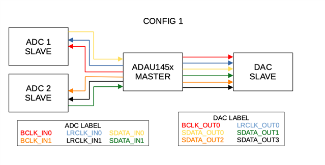
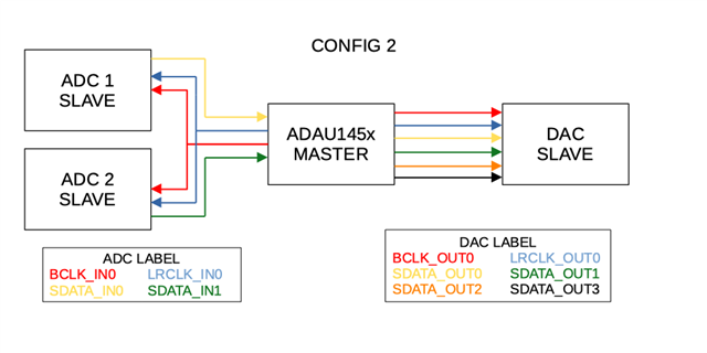
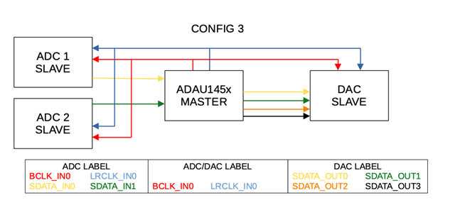
Currently I work in a project which I need connect one ADAU145x with two ADCs and one DAC. So, with you explanations I designed three possible configurations.
In all config the ADAU145x is master and ADC/DAC is slave.
Config 1 : SDATA_IN0 and SDATA_IN1 have its own clock domain signals.
Config 2 : SDATA_IN0 and SDATA_IN1 share one clock domain signal (BCLK_IN0 and LRCLK_IN0).
Config 3 : SDATA_IN0, SDATA_IN1, SDATA_OUT0, SDATA_OUT1, SDATA_OUT2, SDATA_OUT3 share one clock domain signal.
My preferred design is Config 3 because I have 12 General-Purpose Input/Output pins free. I wonder if the config 3 is possible.
Let me know your thoughts about Config 1, Config 2 and Config 3.
Thank you in advanced.
Hello francismariano,
Any of those configurations is possible. It really comes down to your application needs. Our earlier posts on this thread shows that all the serial port clocks will be the same if they are set to master and to the same clock generator output. So if you have three destinations for the clocks, you can use three sets of serial ports or just one set and distribute them to the three parts.
The difference for choosing one over the other is a good topic for discussion. Sample rate and data format will enter into this discussion. Basically, the bitclock rate. If it is high then there is a smaller margin for timing the data verses the bit clock edges. If you are using only I2S, which it seems like you are, and sample rate of 48kHz then any of these will work.
If you are going to run at 192kHz, then PCB layout details like distance between parts and how the traces are run could cause problems with reflections on the clock lines. Taking one clock line and sending it to three devices is certainly possible and often done. If you are going to have high bit clock rates then at least using separate bitclock outputs might be a good idea. You have individual control over drive strength which can be helpful. If you distribute just the LRCLK then you free up the LRCLK pin for the GPIO function.
So if you are using I2S and running at 48kHz then I do not see any problem with configuration 3 as long as the parts are not really far from the DSP on the PCB.
Dave T
Please log in to reply.