Assignment drive strength/slew rate/pulldown register to SDATAIOx-pins is NOT bijectiv
You would assume a bijectiv, simple assignment between the
drive strength/slew rate/pulldown registers and SDATAIOx - Pins:
register F7Bx correponds to Pin SDATAIOx (see datasheet p199).
But this is not the case, you have the following:
F7B0 - SDATAIO0
F7B1 - SDATAIO1
F7B2 - SDATAIO2
F7B3 - SDATAIO3 and SDATAIO4
F7B4 - SDATAIO5
F7B5 - SDATAIO6
F7B6 - SDATAIO7
yes, register F7B3 controls the pulldown resistors of two pins,no way( ?workaround?) to set the pulldown of SDATAIO3 without affecting SDATAIO4?
Fullscreen
StereoAD1937.xml
Download
<?xml version="1.0" standalone="no"?>
<ROM IC="ADAU1467" IC_Address="8" Address_byte_length="1">
<dateTime>2023-11-15T16:03:55Z></dateTime>
<version>4.5.0.1779</version>
<page modetype="Mode 0">
<action instr="writeXbytes" len="2" addr="14" ParamName="CodecADCcontrol0" DspName="IC 2">0</action>
<action instr="writeXbytes" len="2" addr="15" ParamName="CodecADCcontrol1" DspName="IC 2">0</action>
<action instr="writeXbytes" len="2" addr="2" ParamName="CodecDACInit" DspName="IC 2">04</action>
<action instr="writeXbytes" len="2" addr="0" ParamName="CodePLLInit" DspName="IC 2">0</action>
</page>
</ROM>
Fullscreen
DaisyChainAD1937.xml
Download
<?xml version="1.0" standalone="no"?>
<ROM IC="ADAU1467" IC_Address="8" Address_byte_length="1">
<dateTime>2023-11-15T16:03:55Z></dateTime>
<version>4.5.0.1779</version>
<page modetype="Mode 0">
<action instr="writeXbytes" len="2" addr="14" ParamName="CodecADCcontrol0" DspName="IC 2">0</action>
<action instr="writeXbytes" len="2" addr="15" ParamName="CodecADCcontrol1" DspName="IC 2">20</action>
<action instr="writeXbytes" len="2" addr="2" ParamName="CodecDACInit" DspName="IC 2">C4</action>
<action instr="writeXbytes" len="2" addr="0" ParamName="CodePLLInit" DspName="IC 2">0</action>
</page>
</ROM>
EVAL-ADAU1467Z_RevB_SDATAIO_PullDown.dspproj
toggles pulldown of selected register every 2 seconds (needs only a multimeter (0V/80mV) to see pulldowns) .
Audio Signal Processors
ADAU1467 Evaluation board
hardware
adau1467
SigmaDSP Audio Processors
Hello Michael,
I do not know which version of the datasheet you are looking at? It must be an older version? I see two different registers for the two pins.
Page 199 of Rev0 datasheet is for MP24.
Page 199 of RevA datasheet is for the SDATAIO pins drive strength but they do not list them at all and not as the same number.
The screen capture I am showing is on page 98 of RevA and page 96 of Rev0 datasheet.
So where exactly did this list come from?
Also, the code you are showing seems to be for the codecs not the DSP?
Dave T
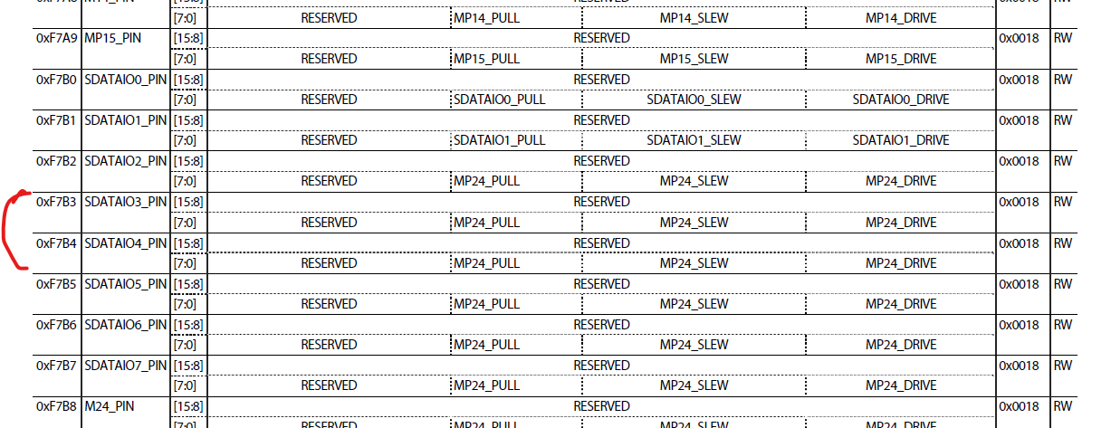
ADAU1467/RevA/p.299 states: "Address: 0xF7B0 to 0xF7B7, Reset:0018, Name: SDATAIOx_PIN" (2nd line)
means:
0xF7B0 : SDATAIO0
0xF7B1 : SDATAIO1
0xF7B2 : SDATAIO2
0xF7B3 : SDATAIO3
0xF7B4 : SDATAIO4
0xF7B5 : SDATAIO5
0xF7B6 : SDATAIO6
0xF7B7 : SDATAIO7
correct is the assignment in my question.
The *.xml is needed to free (force high impedance state) of the SDATAIOx pin on the EVAL-ADAU1467 REV B. - board to verify the assigment with an voltage meter.
Hello Michael,
The list of registers and SDATAIOx pin numbers look good in your recent list.
What question I do not understand is this?
MichaelSchwarzAER said:
The *.xml is needed to free (force high impedance state) of the SDATAIOx pin on the EVAL-ADAU1467 REV B. - board to verify the assigment with an voltage meter
Many of these pins are being used on the eval board. So there are other things hanging on the pin to influence the measurement.
Dave T

Exactly because of this (because "there are other things hanging on the pin to influence the measurement."), you need both *.xml (AD1437) and the attached EVAL_ADAU1467Z_RevB_SDATAIO_PullDown.dspproj. Of course this part of software is only needed on the EVAL_ADAU1467Z_REVB - board to change the AD1437-Pins from output to input to measure the voltage of the SDDATAIOx-pins.
To verify the real, correct assigment you simply compile,link,download the attached ADAU1467 (Sigma Studio 4.7) - program to the EVAL_ADAU1467Z_REVB. With a simple voltage meter you measure the 1/4s(0.25Hz) - alternating 0V/>80mV of the SDDATAIOx-pins. Be sure to select the multiplexer 2x8 switch accordingly in the canvas and don't forget to switch the CODEC BOOT MODE-switch to I2C on the eval board.
Therefore you can verify the correct assigment:
F7B0 - SDATAIO0
F7B1 - SDATAIO1
F7B2 - SDATAIO2
F7B3 - SDATAIO3 and SDATAIO4
F7B4 - SDATAIO5
F7B5 - SDATAIO6
F7B6 - SDATAIO7
(seems definitly not the heart's desire of a DSP-designer).
Hello Michael,
I do not understand what the problem here is?
First let me make a few comments:
MichaelSchwarzAER said:
(AD1437) and the
I think you mean the AD1937 codec?
MichaelSchwarzAER said:
Be sure to select the multiplexer 2x8 switch accordingly
What multiplexer? There is not multiplexer on the board. Do you mean in your program?
MichaelSchwarzAER said:
Therefore you can verify the correct assigment:
F7B0 - SDATAIO0
F7B1 - SDATAIO1
F7B2 - SDATAIO2
F7B3 - SDATAIO3 and SDATAIO4
F7B4 - SDATAIO5
F7B5 - SDATAIO6
F7B6 - SDATAIO7
This list is wrong!!!! F7B3 is not for IO3 and IO4.
This is the list that you had detailed earlier:
MichaelSchwarzAER said:
0xF7B0 : SDATAIO0
0xF7B1 : SDATAIO1
0xF7B2 : SDATAIO2
0xF7B3 : SDATAIO3
0xF7B4 : SDATAIO4
0xF7B5 : SDATAIO5
0xF7B6 : SDATAIO6
0xF7B7 : SDATAIO7
Now, the SDATAIO4 may be a problem. This may be the issue with your measurements??
This is connected to the ASDATA2 pin of the codec which is an output. I am not sure if this actually does float into a high impedance mode? So you will need to remove resistor R16
There is still a test point SDATAIO4 that is available for measurements and connections.
Dave T
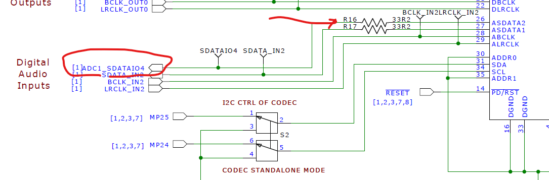
AD1937 of course (I was too lazy to type four digits - sorry).
demultiplexer 2x8 switch on canvas in the program of course (word by word translation from german - sorry).
e.g. the ASDATA2 pin(AD1937 pin 26) is changed from output in an input by the
Dual-Line=Daisy-Chain=TDM-Mode (DaisyChainAD1937.xml)[AD1937 datasheet Rev. B | Page 20 of 36] - no need to remove any resistor.
All you need to verify this non-bijective assignment is a PC running SigmaStudio4.7, the ADAU1467 EVAL BOARD and a cheap voltage meter.
To definitly rule out a deep Sigma Studio bug you can use the default StereoMode of the AD1937((DSDATA4 is an input there) or unsolder AD1937 or using a board consisting of only an ADAU1467), toggling F7B6 in an ultra small loop compiled by hand and see toggling SDATAIO7/MP23(pin 61).
It seems Sigma Studio compiles well in this case. We tested it with several different boards:
Welcome this silicon bug (or better inelegance) of a otherwise really great DSP.
my question: Is there an undocumented routing bit switching between SDATAIO3/SDATAIO4? What does F7B7?
Please log in to reply.