evaluation board layout and gerber details
Please provide EVAL-ADAU1787Z layout and gerber file details for custom design. thanking you .
hardware
adau1787z
pcb layout
gerber files
Hello qds,
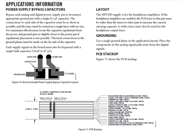
There is a little bit of information in the datasheet about PCB layout. It is in the applications section of the RevA datasheet.
It is just one page so I can actually take a screenshot and put it up here:
I did write up a document a few years back about layout practices with regards to one of our codec products but this applies to any part.
Since I wrote this I also found an issue with a PCB layout where someone tied (connected) the ground pins to the plane for the EP on the top layer. DO NOT do that! It caused the PLL to lose lock because it created a sub-plane with a shorter path that had a bunch of vias (inductors) to ground on the EP which caused ringing that disrupted the PLL lock.
So if a part has an EP then have the EP get its ground from vias to the ground plane but do not connect it to any of the ground plane on the top layer. Keep it on its own.
Now this does not apply to the ADAU1787 since it is a PGA and has no EP. With a BGA you must pay attention to where you place vias. For power and ground pins you need to avoid vias before you can connect it to a bypass cap. So I do not recommend using vias-in-pads for those pins. Usually we design the pinout of the package such that you can bring out the power and ground pins without having to use vias. But, I am not on the design team for all our parts! LOL.
Here is a link to my codec document:
PCB Layout Best Practices for AD193x codecs - Q&A - Audio - EngineerZone
Now with regards to Gerber files.... I do not have any comments about that.
I hope this will give you a good start.
By the way, this all applies to all the parts in your system. Just have it clear in your mind that when you add a via you are adding an inductor and ask if it will cause an issue?
This is the creative part of our jobs!!
Dave T
Please log in to reply.