ADAU1446 errata, delay on SDATA_IN0 and one clocking question.
Dear AD support,
we're in the middle of evaluating the ADAU1446 as a central part of a multi-DSP, multichannel audio solution. After initial tests with the official EVM, we're currently doing measurements of the ADAU1446 on a self built daughterboard that already fits our systems constraints. While most of the ADAU works as expected, we're having four questions/issues, that we would like to get some information on before we can continue developing with this IC.
Q1: We only found one official errata statement:
http://www.analog.com/media/en/technical-documentation/data-sheets/ADAU1442_1445_1446_Anomaly.pdf
... to the ADAU1446 referring to spdif out in silicon rev 0. Is this information still valid, respectively are there really no other known issues in the current ADAU1446 revisions?
Q2: While doing some research for the official errata, I stumbled upon the following article:
Dejitter issue
Needless to say I am more than just interested in the attachment that is missing in that posting. Could you please elaborate?
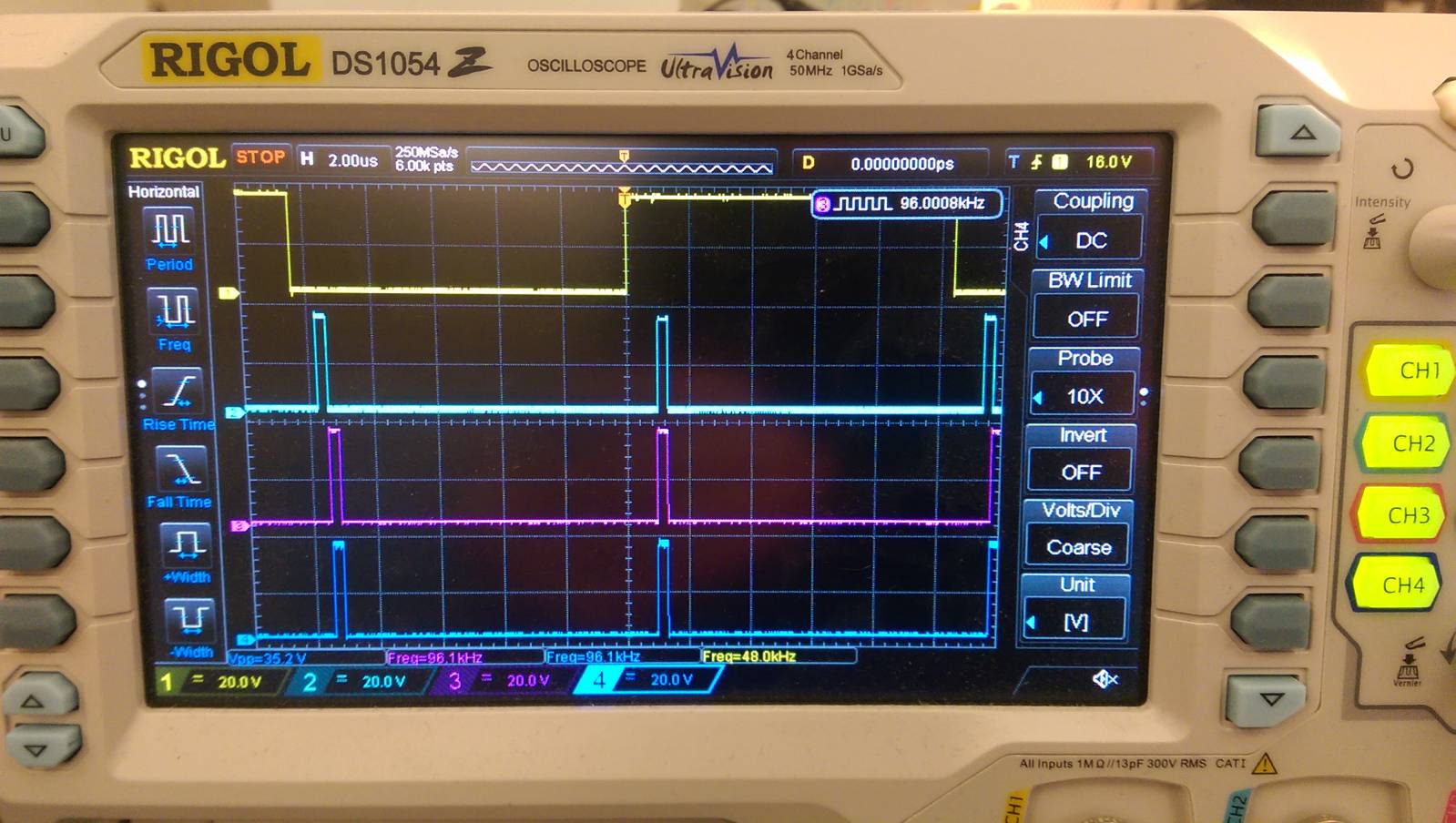
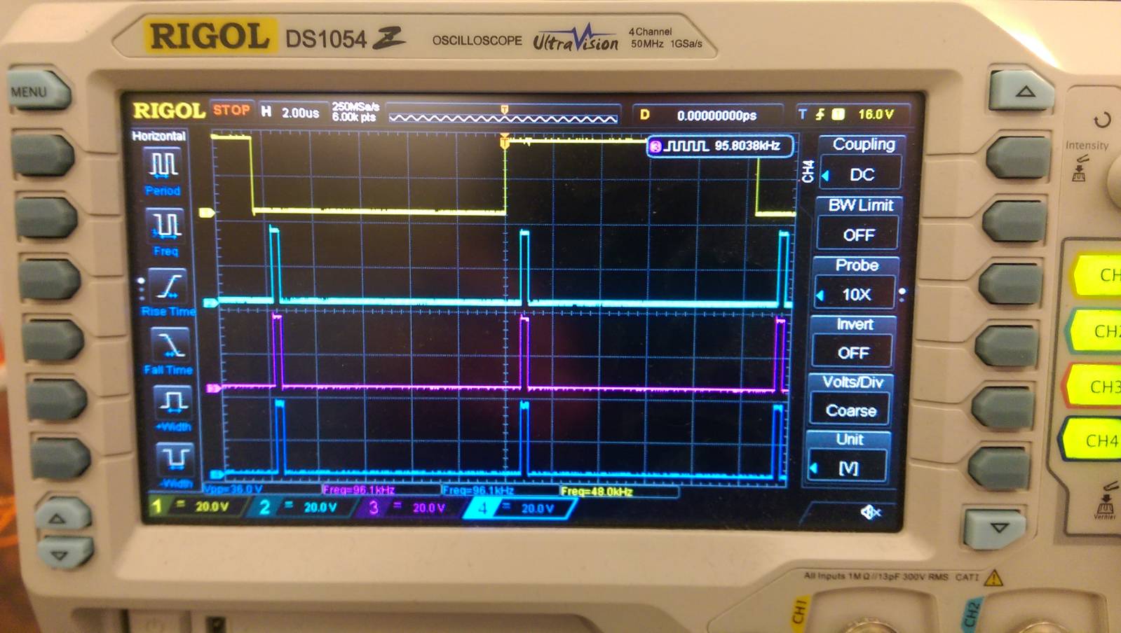
Q3: When using the SDATA_IN0 (Pin 11) in I2S/LJ/RJ/TDM2 mode, the timing of the digital audio passing through the core is not as we expect. The audio data on the left channel is being delayed in time by exactly one sample in respect to all other channels. Using a "walking ones" test signal coming from an APx555 the delay is obvious.
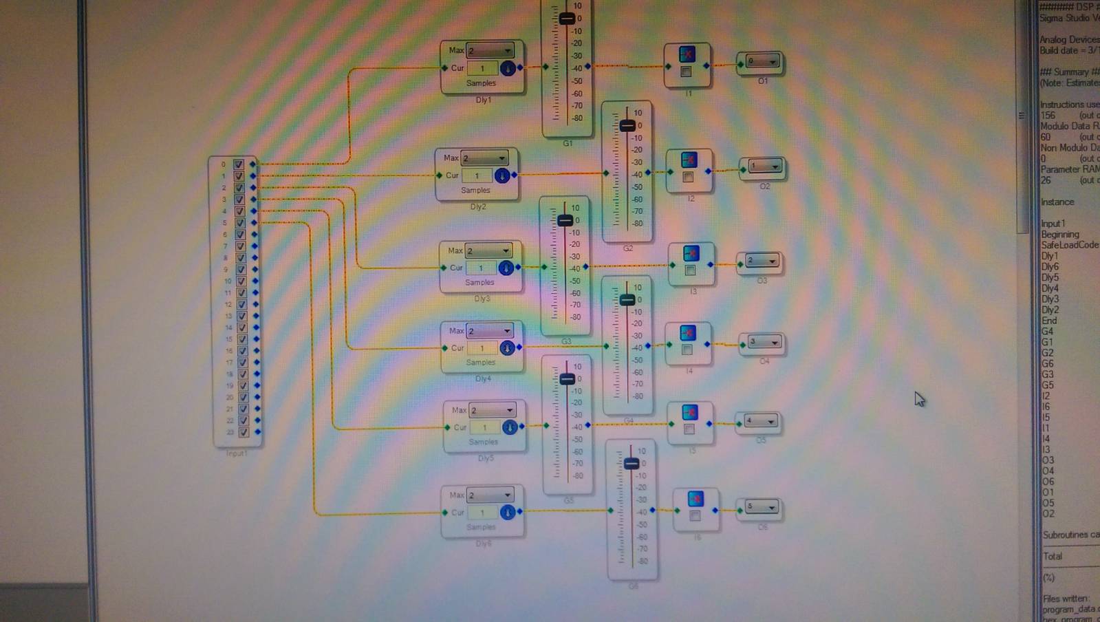
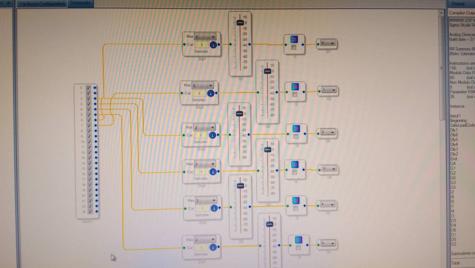
The oscilloscope pic shows the LRCK in yellow, and output SDATA_OUT{0,1,2} in {cyan, magenta, blue}. As the Sigma Studio screenshot shows, this already happens in a pretty minimal configuration.
You can clearly see the (t-1) historical data only on the left sample data on the first of the three I2S data streams. I also attached the routing in Sigma Studio that led to this behaviour (sorry for the heavy moiré):
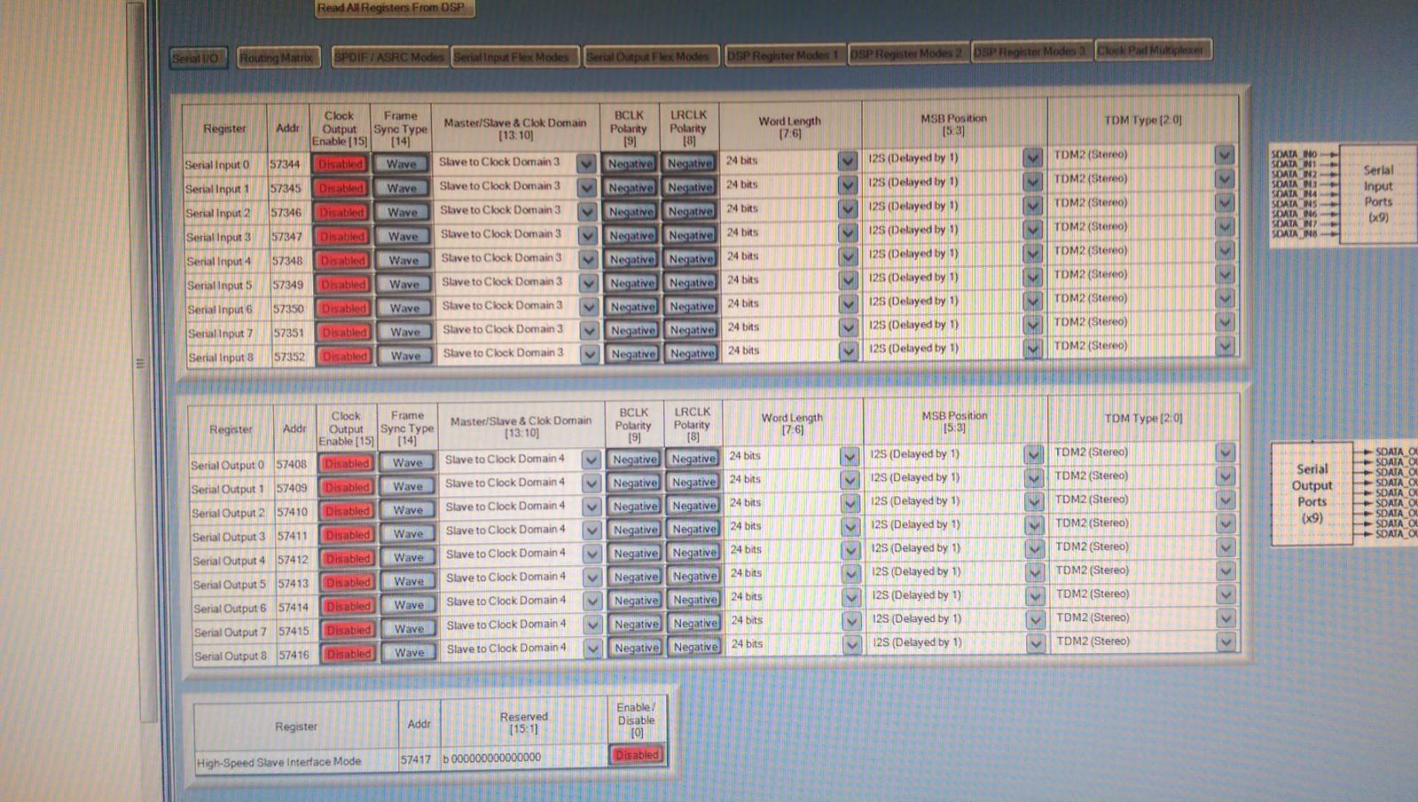
It might help to know we're using three synchronous I2S streams per DSP going into the ADAU using SDATA_IN{0,1,2} and routing them out via SDATA_OUT{0,1,2} using Sigma Studio. Clocking is done by BCLK{3,4} and LRCK{3,4} for {IN,OUT}, a quick picture of the the clock setting in Sigma Studio:
As you can see, all ports are in slave mode receiving the clocks from external clock buffers. Also, we're seeing this issue on two datecodes of the ADAU1446 (#1514 and #1434).
During double checking our testbed, we had to find out that when we just swap the input from SDATA_IN0 to SDATA_IN3 there is no delay on the left pair of channel SDATA_IN. In other words - when we keep everything like it was and only changing the routing to:
... the ADAUs behaviour results in something we would expect:
Q4: According to the current Rev.D datasheet[1] on page 34 ...
"In a system with no sample rate conversion and with serial ports in slave mode, at least two pairs of LRCLKx and BCLKx pins must be connected: one pair for the input serial ports and one pair for the output serial ports [..]."
... and ...
"Although a clock domain in slave mode can clock an arbitrary number of serial ports [...]"
... we assumed that we need two pairs of BCLK and LRCK feeding two clock domains when running the ports in slave mode. So we're currently using BCLK3 + LRCK3 (Pin 3 + 4) for the input "clock domain" and BCLK4 + LRCK4 (Pins 96
+ 97) for the "output clock domain". As this is a synchronous design, both BCLK and LRCK inputs are fed by a plain buffered copy with a very low, single digit ns skew (measured)). When selecting _only one_ of these BCLK/LRCK copies in Sigma Studio as clock, audio still passes through as with both clock pairs before. Does this mean we can safely omit one of these clock pairs in the final design? If so, why do you recommend two pairs of LRCLKx and BCLKx pins?
Kind regards,
Daniel
[1] http://www.analog.com/media/en/technical-documentation/data-sheets/ADAU1442_1445_1446.pdf
Audio Signal Processors
adau1446
adau
SigmaDSP Audio Processors
SigmaDSP
Hello Daniel,
Thanks for your great post with plenty of detail! I will handle these one at a time:
Q1: We only found one official errata statement:
http://www.analog.com/media/en/technical-documentation/data-sheets/ADAU1442_1445_1446_Anomaly.pdf
... to the ADAU1446 referring to spdif out in silicon rev 0. Is this information still valid, respectively are there really no other known issues in the current ADAU1446 revisions?
There are very few things we have uncovered in the years since this part was designed. I will go from memory here to attempt to list them.
This SPDIF issue is still there. It was fixed in the ADAU145x and newer products.
There is small issue with the ASRCs lock bit register. It is sticky, a little too sticky in that it will show when you obtain lock and then never reset again even if you have lost lock. So it is not a good representation of a signal being present. This was also fixed on the ADAU145x and newer products. Of course, this does not apply to the 1446 since there are no ASRCs.
Then there is the dejitter issue you mentioned. Details below...
Q2: While doing some research for the official errata, I stumbled upon the following article:
Dejitter issue
Needless to say I am more than just interested in the attachment that is missing in that posting. Could you please elaborate?
Thanks for finding this. This was one of many posts that were migrated from an older version of EngineerZone and the attachment obviously did not follow it. I was able to find it in our archives so if you go to the post now you will see the attachment.
Now you should know that SigmaStudio will change the dejitter window for you after every link/compile/download. So if you go into the register settings and set it to zero it will change it back to 5 when you compile. It will actually change it to zero then to 5 and you cannot change that. If you have a system controller then you can go in there directly and change it. You can also do it from SigmaStudio after you compile by going to the register and writing a new value.
Q3: When using the SDATA_IN0 (Pin 11) in I2S/LJ/RJ/TDM2 mode, the timing of the digital audio passing through the core is not as we expect. The audio data on the left channel is being delayed in time by exactly one sample in respect to all other channels.
This is a new issue that I have not seen. I will not be able to set this up in the lab today to look for a work-around. Since you have it setup can you try changing the dejitter window settings to see if this changes the behavior?
Can you also attach the project you are using that show this problem? This way we can work directly from the exact setup you have.
Q4: According to the current Rev.D datasheet[1] on page 34 ...
"In a system with no sample rate conversion and with serial ports in slave mode, at least two pairs of LRCLKx and BCLKx pins must be connected: one pair for the input serial ports and one pair for the output serial ports [..]."
[...]
Does this mean we can safely omit one of these clock pairs in the final design? If so, why do you recommend two pairs of LRCLKx and BCLKx pins?
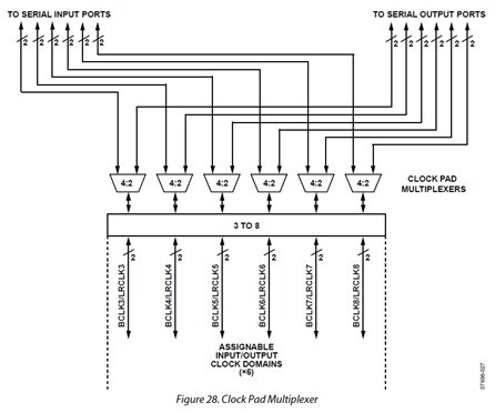
No, you cannot omit one of the pairs. Look at figure 28 in the datasheet. This shows the routing very well.
You can see the 4:2 Muxes that route the clocks coming in/out from the pins and connecting them either to the input serial ports or to the output serial ports but not both. So if clock domain 3 is going to the input ports it is not going to the output ports. So another domain is needed to send the clocks to the output ports.
Now sometimes I have seen the input or output ports function when there appears to be no clocks being sent to it. I usually attribute this to noise in the system that is triggering the shift registers or there could be some crosstalk inside the part when a floating line is selected as a clock source. So the basic situation here is that you must jumper your clocks to two domains so that one can be assigned to the input ports and the other to the output ports. I really do not know why the designers chose to do it this way as opposed to sending it to both at all times. There must have been a reason.
Let us know how your tests are proceeding and if you have further questions.
Dave T

Hello Dave,
thanks for your quick and comprehensive answer! So good to hear there's not much known about the ADAU1446 (Q1).
The dejitter circuit errata (Q2) will not be a problem for us, since our clocks and signals measure perfectly in spec, so we'll probably just disable that feature, especially if it has to potential to reduces reliability. The behaviour of Sigma Studio considering the dejitter configuration part appears a bit strange to me, but we're using it only during development or when things do not behave as expected. Most of the time we're generating "the configuration" ourselves and dump it into the DSPs via SPI or simply change the plain registers to fit our needs, so this won't be a problem.
While I honestly don't like the idea of intra-IC crosstalk being the reason for the "unclocked domain" to work (Q4), it is a feasible explanation. During our tests, we simply switched the clock domains for input/output to the same within Sigma Studio, but we did not ground the second input of the ADAU. So I'd say figure 28 in the datasheet clearly misses the crosstalk path between the adjacent 4:2 muxes 8)
Anyway Q3 (unwanted input delay on SDATA_IN0) remains a respectable issue, in the meantime we could reproduce our measurements of the delayed sample on the EVAL-ADAU1446EBZ as well. We also did some more measurements and found the issue to happen when choosing TDM4 as the input format for SDATA_IN0.
So as a summary, every ADAU1446 DSP in our lab delays the first sample of an incoming stream on SDATA_IN0 by one. It happens consistently with all sample frequencies we tested (10kHz ... 100kHz), it's as if it was multiplied by z^(-1). We could not find any correlation between that unwanted delay and the settings of the dejitter register. I attached the minimal example of a Sigma Studio project you asked for to get you started. The source of the test signals was the APx555 again, the issue does not occur when we avoid SDATA_IN0 and use SDATA_IN3 instead.
Kind regards,
Daniel
Please log in to reply.