Problems setting PLL up on ADAU1452
I am unable to get my custom ADAU1452 board PLL locking. The MCLKIN/OSCIN is driven by a crystal oscillator IC at 3.3V and it looks good on oscilloscope. Checking the PLL lock register never shows lock. I am able to write to the target i2c control bus to other registers, but it seems like the PLL_CTRL0, PLL_CTRL1, MCLK_OUT, PLL_CLK_SRC don't really update when given write commands:
Here is a transcript of what I am seeing:
# Soft reset on
write 0 0xf890 2 0x0000
read 0xf890 2
> 0000
# Soft reset off
write 0 0xf890 2 0x0001
read 0xf890 2
> 0001
# PLL_CTRL0
write 0 0xf000 2 0x0060
read 0xf000 2
> 0060
# PLL_CTRL1
write 0 0xf001 2 0x0002
read 0xf001 2
> 0000
# PLL_CLK_SRC
write 0 0xf002 2 0x0001
read 0xf002 2
> 0000
# MCLK_OUT
write 0 0xf005 2 0x0005
read 0xf005 2
> 0000
# PLL ENABLE
write 0 0xf003 2 0x0001
read 0xf003 2
> 0001
Is it expected that the readback of these values is not reflected immediately (datasheet says they take effect only on the subsequent call to pll enable). I do notice the PLL enable seems to stay with 0x0001 for a few seconds but then goes back to 0x000. I tried two separate chips in the same board, so I don't think it is a chip failure. Though the PLLFILT voltage seems to be 3.3V which is higher than the ~2ish or so that was quoted in the forum previously. Writing to other registers like the soft reset and the program memory seems to work fine... here's a transcript to writing 0xc000
write 0 0xc000 10 0xABCDABCDABCDABCDABCD
read 0xc000 10
> abcdabcdabcdabcdaaaa
write 0 0xc000 10 0x1234567890ABCDEF0123
read 0xc000 10
> 1234567890abcdefaaaa
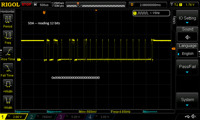
The i2c signals look to be sufficient signal quality (I've attached an oscilloscope capture of the SDA). I'm really out of ideas, so I'd appreciate some advise. I've also checked DVDD, PVDD, IOVDD voltages and they are 3.3V, 1.2V, and 3.3V respectively.
Audio Signal Processors
adau1452
Datasheet/Specs
i2c
SigmaDSP Audio Processors
pll
Show More
Hello Andrew,
I think the problems you are having is related to timing of your startup routine. There are a number of small details that need to be addressed.
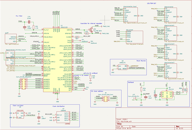
Before I get into that I see the XTALOUT pin has a label on it but I do not see if you actually attached it to anything. Since you are using a Clock-Osc I would not tie that pin to anything and I think you are not connecting it anywhere.
OK, the startup routine is a little tricky.
First, you cannot use a high SPI clock speed for the SPI comms until the PLL is locked. The part is using the signal that is feeding the input of the PLL. This is the crystal output but it is being divided before the PLL. The Prescale divider defaults at power up to divide by 1. But, if you are doing a warm boot this will most likely be dividing by 4. So keep the SPI speed below 3MHz until the PLL is locked.
The other detail is that these registers are shadow registers. They only are transferred to the real control registers when the PLL enable goes from zero to one. IF you write to these registers when the PLL is enabled nothing will change. You have to disable and reenable the PLL for the updated value to actually be updated! This includes the CLKOUT pin.
I suggest you study page 30 and 31 of the datasheet. This is the power up sequence.
I see you are doing a soft reset. This is good because it resets the registers to a known value.
You will need to make sure your power rails are up to full voltage.
Then I see you have an enable pin on the OSC. This needs to be enabled right away after power up or right at power up.
Then, you will see in the datasheet that once all the power is good and the oscillator is there the part will run some code for 650ns. This is not a very long time but there is a chance you might be writing too early after you did the reset.
The other little detail is that you cannot write to these registers if the core is enabled. Also, when the PLL is attempting to lock the control ports are inactive. So there are a lot of little pitfalls here to mess you up.
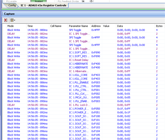
Have a look at the capture window of SigmaStudio for a hint at what you should be doing with your controller:
It first sets the port into SPI mode with the three toggles of the SS pin.
Then it sends the Soft Reset like you are doing.
The it executes a delay ( a wait time) of 0xFF milliseconds. That is 255 milliseconds.
Then it kills the core.
Disables the PLL
then finally writes to the PLL registers.
Then it waits another 255 ms for the PLL to lock.
In this case you could read the lock bit register and you could wait less time because the PLL will lock much quicker but 255ms for us humans is not very long.
Then SigmaStudio starts writing to the other registers and then the program RAM and Parameter RAM and then starts up the core and away you go!
The PLL Filt voltage is telling you it is at the max end of the range of the VCO and it is trying to lock to a signal. I do not recall if a higher voltage produces a lower VCO frequency? This would mean it is trying to match a 0Hz signal. If it is the other way then perhaps you might not be correctly setting the prescaler due to the issues I mentioned above and it is trying to match a frequency that is too high for the PLL to lock to.
But, I think you are running into issues with the sequence. There is also possible PCB layout issues but again, I do not think this is the problem. This PLL works well and locks easily. I have seen it lose lock if there is noise and poor PCB layouts but it still usually locks for most of the time.
Dave T
Thank you for the detailed reply.
DaveThib said:
First, you cannot use a high SPI clock speed for the SPI comms until the PLL is locked. The part is using the signal that is feeding the input of the PLL. This is the crystal output but it is being divided before the PLL. The Prescale divider defaults at power up to divide by 1. But, if you are doing a warm boot this will most likely be dividing by 4. So keep the SPI speed below 3MHz until the PLL is locked.
I am using I2C not SPI to control the part. It's pretty slow (i'm running like 25khz of bitbanged i2c). I assume most things are the same. I've tied SELFBOOT low, but even in selfboot I have the 10k pulldown SS_M/MP0 (26). Are you suggesting it is not possible to set the PLL settings w/o SPI?
DaveThib said:
Before I get into that I see the XTALOUT pin has a label on it but I do not see if you actually attached it to anything. Since you are using a Clock-Osc I would not tie that pin to anything and I think you are not connecting it anywhere.
While I labeled it, it is not connected to anything as you suggest.
DaveThib said:
You will need to make sure your power rails are up to full voltage.
I wait many seconds before trying to program anything. I'm doing this semi-manually so the inherent delayar probably in the second range. I also have enable on the oscillator tied to v33, so it starts as fast it can, probably faster than the adau1452 comes out of reset, because i have a reset supervisor chip on the adau1452. The only hardware thing I might check is if replacing my ferrite beads that are isolating the power-rails with 0 ohm resistors fixes the problem. Somebody else posted similar problems as me and it turned out that JLCPCB had incorrectly populated resistors where they wanted FB.
DaveThib said:
But, I think you are running into issues with the sequence. There is also possible PCB layout issues but again, I do not think this is the problem. This PLL works well and locks easily. I have seen it lose lock if there is noise and poor PCB layouts but it still usually locks for most of the time.
I will try being much more precise in my sequencing, and see if I can resolve my problem. The answer about the shadow registers helps a lot, because that was confusing me quite a bit.
Thank you again!
Hello Andrew,
I did not notice you were using I2C. So many people (most) use SPI that I just default to it but the chip defaults to I2C. I2C is so slow that it is usually not a problem with the clock speed before the PLL is locked. So that is good.
However, the other delays when resetting the part and setting up the PLL etc., are very important. You will read that in the datasheet.
Ferrite beads can cause ringing issues on the power and ground lines. So far I do not think this is a problem but down the road it might be. So I would agree to replace them with zero ohm resistors. That is strange about JLC. I have used them as well for a few projects here but mostly for my personal playing around projects. (Yes, I love my job so much that I do this for fun as well!) LOL
Look carefully at the sequencing.
Also, I just noticed something in your schematic. The EEPROM is a 24LC32. That is a 32Kbit EEPROM. That is super small!!! It will only hold 4k bytes of data. You will max this out easily. Shoot, there are a few hundred registers and they are mostly 16 bit registers and then the address is 16 bits so right there you use four bytes per register (although often they are loaded in burst mode so the address is automatically incremented. ) Then you have all the 32 bit parameter memory and 32 bit program memory. You will max out this EEPROM quickly!!
We have a 1024 kbit EEPROM on the eval board and you might be able to get away with a 512kbit but a 32 kbit will just be too small.
What will happen is that SigmaStudio will try to program it and the data will wrap around and overwrite the older data. So then the chances are the first byte will not be an 0xAA so the part will not selfboot. It will fail when it does not see the 0xAA at address zero.
Dave T
Thanks for all the help, things are going great now, but I wanted to report back to help any future people who have the same problem.
Sorry for the long delay in replying, but I found the root of my problems--basically my power rail had too low of voltage. I was supplying my board with 5V regulated from my lab supply, but there's a schottky diode witha .4V dropout. When the power draw went from reset to PLL enabled (and later program execution), the voltage dropped past the 3.3V regulator's threshold. That being said, I think through the course of your advice I fixed several other things that might have been causing me problems like the sequencing, delays, and decoupling.
I discovered this, because I had rev'd the board to a 4layer instead of 2layer, which allowed me to give better return path for some of the higher frequency signals. I also improved the decoupling capacitor escaping from the chip to match the very nice and detailed datasheet. Since the new board was much better but had the same symptoms, I discovered the true root cause of my problems.
Thanks for seeing the EEPROM size problem. I haven't used self-boot on any my designs, so that was just there on a whim, but if I do use it, I'll put a bigger EEPROM.
I've been able to prove my board out enough to get SPDIF in and TDM8 output to 4 TAS5754M TI digital amplifiers. I'm running the TDM signal on a multitapped ribbon cable, and I had a bit of signal integrity issues on the last one, so I might have some transmission line ringing. I suppose it might have been better to make multiple separately buffered I2S ports for each amplifier rather than running them in a bus. By increasing the slew rate and drive strength on the TDM lines, the signal integrity seems sufficient now. (I'm running a SCLK of 12Mhz to give 256fs so I can do 8 32 bit channels). I just threw some 22 ohm resistors close to the output pins, so I'm not doing any brilliant termination.
Hello Andrew,
Glad you have made some great progress. Yes, running TDM8 with a 12MHz bit clock can be challenging if you have to run it over a ribbon cable. I usually try to alternate the signal wires with ground wires so the ribbon will have signal, ground, signal, ground... which gives the signal a defined impedance and a defined return path for parasitic currents. Even then, the added capacitance can cause issues so the shorter the better and you are correct. If possible avoid TDM8 and go with multiple I2S lines and a 3MHz clock.
Glad you knew to go to the drive strength registers.
Hope the rest of your project goes smoothly.
Dave T
Please log in to reply.