ADAU1701 No Response
Hello,
I have a custom designed board using the ADAU1701 DSP, the board uses a Texas Instruments TM4C processor to put the DSP into SPI mode and load data into it.
I am not getting any response from the DSP, I am not even certain its PLL ever locks on the clock. I have been closely following the procedures and recommendations in the datasheet for the device. I have verified the signal levels and voltages for all the pins, including the SPI pins.
I had problems with the oscillator, I ordered an AT-cut crystal (Abracon ABM3-12.288MHZ-D2Y-T) with 18pF load capacitance. Based on the formula in the datasheet, I computed the oscillator capacitors to be around 27pF. This setup never appeared to work. I could see the ADAU1701 OSCO pin ringing the oscillator, but the MCLKI pin just had a DC offset, no oscillation. I am assuming this is not normal. I swapped out the crystal for a new one, I also swapped out the capacitors for 22pF as shown in the ADAU1701 datasheet schematic. The oscillator never worked.
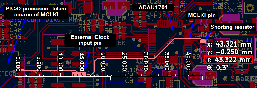
The PCB was designed with a 0 Ohm resistors in the oscillator traces to allow for an external MCLKI signal to be injected. Obviously, the oscillator and the external MCLK were never used simultaneously, the shorting resistors were removed when the external clock was connected, to isolate the crystal and it's capacitors.
Even with the crystal/capacitors removed, and an external 12.288MHz clock supplied to the MCLKI pin (from a signal generator with good stability), the chip never woke up.
I have 2 suspicions for what's wrong, but I would like to hear other professionals input before I make assumptions.
The MCLKI PCB trace is causing an impedance mismatch that doesn't allow the crystal to oscillate, or doesn't allow a clean sine wave to be present when using the external clock source. This is causing the PLL to trip and never lock. The PCB trace is approximately 43 mm in length. The crystal and capacitors, as well as the shorting resistor are right near the MCLKI & OSCO pins, but the MCLKI trace to the external connection clock input is always wired. So even when the Crystal is used with no external clock input, there is a 43mm trace on the MCLKI pin that leads to an open.
just as a note, I have added significant delays after power-on, and a reset signal, to give the device time to boot up and lock. Far exceeding the maximum durations listed in the datasheet. I don't think the problem is with not giving the DSP sufficient time to wake up.
Note: the PIC32 is inactive, it is for future use after successful bootup of the ADAU1701
2. Suspicion #2 is that the DSP was damaged during soldering. I used lead free solder that has a higher melting point, and had to crank up the hot plate to 300 degrees (C). I know this is always a risk, however I have done the same procedure with AD1452 and the AD1938 and they did not suffer any kind of damage, nor has any other chip I have soldered with this paste.
3. Is it possible that I don't understand the MCLKI pin behavior? Is the clock input actually supposed to be on pin OSCO, and MCLKI is supposed to look like DC?
I have two options moving forward, I can desolder the ADAU1701, sever the MCLKI trace and use the crystal only. Second option is to condemn the ADAU1701 and replace it (I have a spare).
I am reluctant to think that the DSP is broken, as mentioned before, I can see on my oscilloscope the OSCO pin is trying to ring the crystal. The VDRIVE pin is correctly biasing the transistor to generate the 1.8V for pins 13/24. The MP2 pin is connected to an LED for indication, and I can see that it's powering the pin as part of the default MPx state.
It feels like the DSP is alive, but it's just not accepting the program or not responding to SPI commands. ADDR0 is tied to GND, so the chip address should be 0b0000000, and the WRITE command is 0, so the first byte for an SPI write should be 0x00.
PLL MODE 0/1 pins are hard wired to GND and 3V3 respectively. There is a 600ms delay that does nothing to allow the DSP time to boot up, there's another 600ms delay after the RESET pin is toggled from HI to LO and back to HI. After the waiting period, the CLATCH pin of the ADAU1701 is toggled HI to LO 3 times, and a few ms later the first transmissions are sent.
I've looked at the SPI bus with a logic analyzer, the clock transitions, CLATCH, etc all look to be okay, they're following the required polarities in the datasheet. But there is never any output from the DSP COUT pin. The pin stays low throughout the entire time. Changing the command to 0x01 to read from the interface has no effect. I tried several single and burst reads from both the program and parameter rams, but they're "empty" after writing to them.
It looks like the DSP is not entering SPI mode and I'm just transmitting data into the ether. All I can think of is that the device is not initializing properly. I've worked with the AD1452, AD1938 before, and they worked successfully, but this one has me stumped.
Audio Signal Processors
dsp
Datasheet/Specs
spi
Integrated/Special Purpose A/D Converters
clock
SigmaDSP Audio Processors
Audio CODECs
adau1701
Show More
Hello Ernastovich, All assigned engineers are out of office currently. DaveThib will be back in the week of 1/5/2026 to answer your question!
ADI North America will be on winter shutdown starting December 24, 2024; perhaps another community member can assist you until our return on January 2, 2025.
Hello Ernastovich,
As you might guess, I have a huge backlog of posts and email on my first day back after the break. So I apologize that I did not read every little bit of your post like I usually do. I usually read it several times
. This is strange, The MCLKI pin goes into the part and splits. It goes to the PLL input and then it also goes to an inverting buffer. This buffer causes a phase shift and of course the inversion, creates an oscillator when a crystal is attached. So the fact that you see something on OSCO pin and nothing on MCLKI pin is quite strange! With nothing coming into the MCLKI pin then the PLL has nothing so it would not be functioning and hence no way to communicate to the part.
I would like to also hear what you have connected to the PLL Loop Filter pins.
Can you attach your schematic of this part of the design? The crystal circuit and the PLL Loop filter circuit?
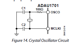
Why is there nothing on MCLKI pin? This has nothing to do with the DSP. It is purely an input. Is there a short to ground? Is the cap (C2 in this diagram) shorted??
You did mention changing the crystal and the caps. Shut off the power and see what you have for resistance to ground from the MCLKI pin?
Is there a short to the PGND pin? It is the pin right next to the MCLKI pin.
Enough questions for now.
Dave T
Dave,
Thank you for the response. Sorry about the delayed response to your questions. I made a decision to tear up the old board and remake it since the PCB house sent me 5x at a time.
The device ended up working with my schematic, so everything is okay. It was just abhorrent soldering that caused little solder spheres to coalesce and hide behind the pins causing all sorts of havoc. Couldn't see them with my microscope at first
Thank you for the support!
Hello Ernastovich,
Thanks so much for letting us know what you found and how you solved it. This may help others in the future!!
What a mess you had to deal with!!! That is horrible!! I could also see that you might get a unit to work then ship it out and a sphere comes loose and the customer gets it and it does not work or worse, goes up in smoke!!
Hope the rest of the project goes well,
Sincerely,
Dave T
Please log in to reply.