How to route TDM audio through multiple ADAU1701s?
Hello all,
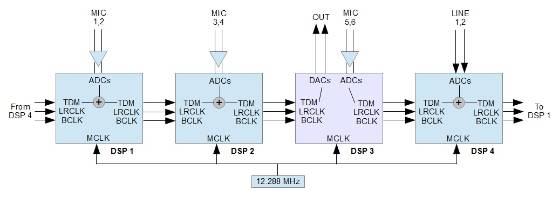
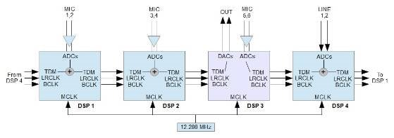
We're developing an audio mixer around a ring of ADAU1701s where each receives a TDM steam from its neighbor, adds in two analog inputs and sends the mix through to the next -1701. The block diagram below shows four -1701s, we plan to use six to accommodate all the needed inputs. One of them ("DSP 3") is programmed differently to break this ring -- handling the first inputs while converting the mixed outputs to analog. We're using TDM because several streams are needed for mix-minus, a headphone bus, etc. The -1701s would also perform some audio processing such as EQ, all booted and directed by a PIC microcontroller via two I2C buses.
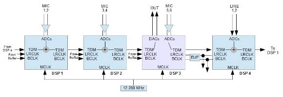
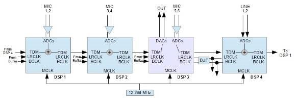
This is where it gets confusing. I'm assuming first of all that all the TDM outputs would be set up as masters, all inputs would be slaves, and the each output's clocks would feed the next input (as shown above) except of course for MCLK which is synchronous to all. Mike who is designing the unit and who is more comfortable in the "digital snake pit" than myself, would like to see all the clocks synchronous as shown below -- as this would mitigate any accumulated timing errors:
I have no idea if either or both setups would work, or could there be an entirely different way to approach this design. Any suggestions would be appreciated. We're using multiple -1701s because one of these performed so well in our first product, and we like having the analog I/Os built in.
Best regards,
Bob
Audio Signal Processors
bclk
lrclk
master
mixer
SigmaDSP Audio Processors
tdm
slave
adau1701
Show More
Hi Bob,
According to my background experience, both of these setups would work. I don't see any real advantage or disadvantage to either approach, other than the following: in the situation where all clocks are synchronous (option 2), you need to make sure the hardware is designed such that there is enough drive strength on the LRCLK/BCLK signal sources to drive 4 slave ICs. That might require extra hardware in the form of clock buffers to deal with the fanout.
Option 1 has the advantage that each ADAU1701 is perfectly capable of driving one slave device from its master I2S port. No problem!
Also, remember that when you approach the problem from the point of view of latency, this is an unavoidable issue: the serial ports and DSP of every device will have latency, regardless of whether that device is a master or a slave. By daisy chaining multiple devices in a serial fashion, latency will accumulate. That is unavoidable. Neither Option 1 nor Option 2 will mitigate this problem. You'll probably want to include delay cells in the SigmaDSP code to appropriately delay the analog signals received in DSPs 2, 3, and 4 to properly align them with the analog signals received by DSP 1.
So, now that I have talked this through, I think I actually prefer option 1 because it potentially simplifies the hardware by avoiding the need for additional buffers.
I would be happy to continue this discussion. Please post any follow-up questions if you have any.
Hi Yagami,
Thank you for your thoughtful answer and your invitation to post additional questions -- which we'll do as they come up while this project advances.
Best regards,
Bob
Hi Yagami,
Our prototype has one of the 1701's feeding buttered LRCLK and BCLK to all the others (the second option above). The TDM bus is working well, with the various signals entering and exiting where needed much like cars on the Capitol Beltway. When my friend Mike lays out a board, it's art.
Best regards,
Bob
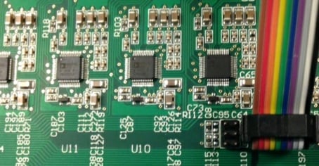
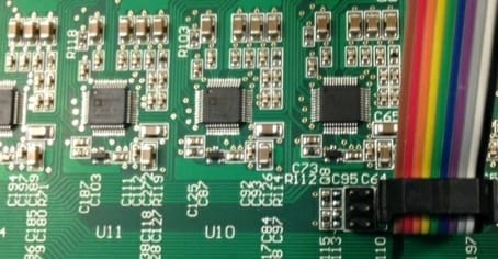
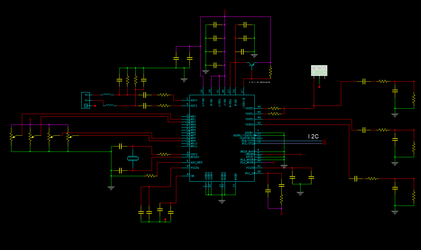
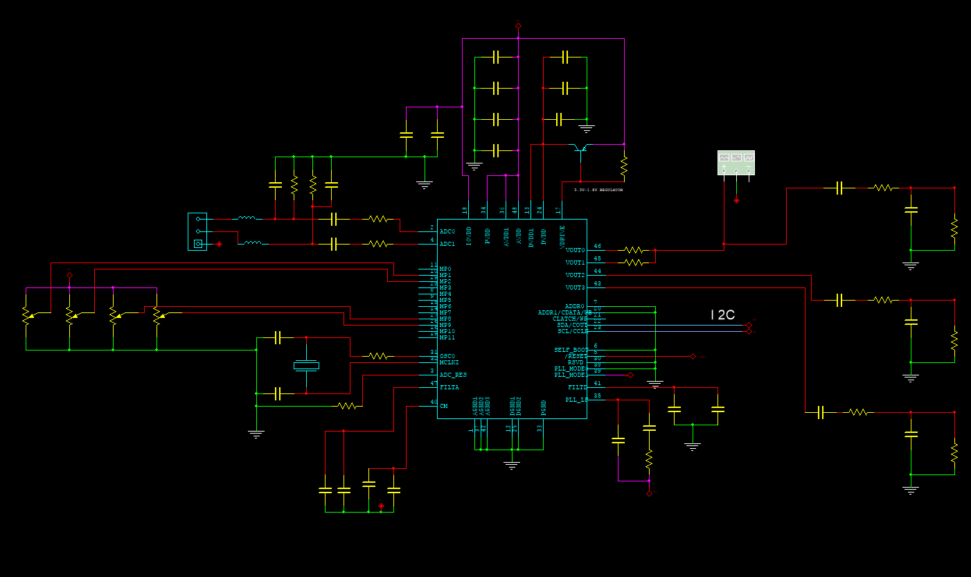
Can I run 2 ADUA1701 in parallel as shown in the link independent of each other for a left and right Channel ? I intend to use the four pots using the 4 ADC for Frequency, Q, Gain, and a line trim for each channel ..
will there be any delay between channels 1 and 2 ?
circuit link on page 50
http://www.analog.com/static/imported-files/data_sheets/ADAU1701.pdf
Thanks in advance
Hello,
The ADAU1701's analog-in to analog-out delay (latency) is about 1 mS at 48 KHz sample rate. Because this is primarily from the oversampled digital filters within the ADC and DAC, it should match between chips.
Best regards,
Bob
So if I build 4 interdependent units that uses it own clock microphone 1 would be 1ms delayed behind microphone 2 ?
1 ms is not noticeable to humans , and how would I sink them ?
Thanks
Hello,
If each of the four -1701s is processing an independent signal (that is, one's output does not feed another's input), then signals arriving at the DSPs simultaneously will output together (except for any differing delays you put in the programs). If you intend to run the DSPs in cascade (as shown at the top of this thread) it would be better to link them via I2S. This avoids multiple conversions.
If your DSPs are on the same board, sync them by supplying their MCLKI (pin 32) inputs from a common 3.3V packaged oscillator. Place series resistors close to the oscillator as shown at https://ez.analog.com/message/130241#130241
Bob
is there any advantage/disadvantage for each unit have it's own clock and e prom ?
The only thing is common in this design is the power supply is there any advantage/disadvantage ?
Hello Bob! Real nice one with 4 ADAUs standing in a row) lifts up spirits for sure)))
Could you please further clarify with master clock sync between the ICs? I'm thinking of a design with just two ADAU1701s (1401A in fact) with the main purpose of separate processing of 2 stereo channels but also I'm thinking over the possibility to send I2S or TDM (depends on which is easier to implement) from one ADAU to another in a situation where 4 analog outs suffice but a processing chain I want needs more processing power than one chip can give.
So my question is what do you think about the solution of getting MCLK for the second ADAU from the BCLK output of the first one (MP11 pin), as it is suggested in the datasheet (p. 18, "using the oscillator")?
The second method is to use a clock from the serial output port. Pin 19 (MP11) can be set as an output (master) clock divided down from the internal core clock. If this pin is set to serial output port (OUTPUT_BCLK) mode in the multipurpose pin configuration register (Address 2081) and the port is set to master in the serial output control register (Address 2078), the desired output frequency can also be set in the serial output control register with the OBF[1:0] bits (see Table 49).
If it is a workable solution what would be the best way to implement it?
If still the external "3.3V packaged oscillator" as in your project is a better way to do the job, could you please explain why, and show some link to the device in question?
Anyone who can comment on this, please welcome)
Hello Ivan,
We use a Abracon ASFL1-12.288MHZ-EC-T oscillator. Since we're driving six DSPs we buffered its output with a SN74LVC2G34DBVR. The BCLK method should work but as I haven't tried it, it would be better for someone who has done so to comment on implementation. One advantage of going with a packaged oscillator is that the sometimes frustrating task of getting a crystal to oscillate reliably has already been done for you.
Best regards,
Bob
Yagami noted above that there would be latency accumulating in the various signals as they travel across their TDM paths between each DSP. Recently I measured this delay on the prototype mixer, it amounts to three (3) sample intervals per TDM link. For my farthest signal five chips away, that works out to 15 samples, or 0.31 mS.
Bob
Please log in to reply.